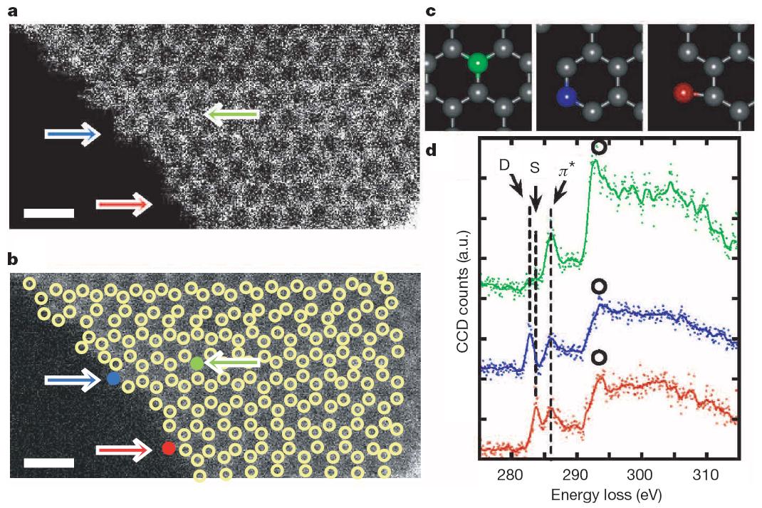
Following this year’s Nobel prize in physics to Andre Geim and Konstantin Novoselov, the relevance of graphene hardly needs to be stated. Graphene-based devices have a real potential owing to the material’s unique electronic properties. If graphene, which is metallic, is cut into small pieces it becomes semiconducting and could be used as a transistor. The problem is however the edges of such small graphene devices. These perturb the operation of graphene transistors, and this is the reason one has to be cautious when it comes to immediate relevance for applications.
To figure out what exactly happens with atoms at the edges of graphene, Kazu Suenaga and Masanori Koshino from Japan’s National Institute of Advanced Industrial Science and Technology imaged and characterized the electronic properties of single atoms at the edge of graphene with a high-resolution scanning electron microscope. Their findings on how these atoms bond with each other are published this week in Nature.
When it comes to transistors that are smaller than anything that could be done with silicon, graphene is one of the materials of choice. As transistors shrink so much they consist of only a few atoms the electric currents that atomic bonds have to carry can become huge. Only a few materials can sustain this and graphene would be perfect for it. “The bonds between the carbon atoms in graphene are very strong and can carry exceptionally high currents,” Andre Geim told me once when researching a feature on future computing technologies. Moreover, electrons can travel through graphene for long distances, easily comparable to the distance between the source and drain electrical contacts of a transistor. “Your electrons would move between source and drain without scattering,” says Geim.

Characterising individual atoms of graphene. The atoms depicted in red, blue and green colours represent atoms at different positions on a graphene sheet. Their energy loss spectra mirror their different properties. Reprinted by permission from Nature doi: 10.1038/nature09664 (2010).
While all this is true for the centre of graphene sheets, the edges are a different matter. There, electrons scatter and all these nice benefits of graphene are diminished. And the smaller the transistors get the more edges there are in relation to the rest of the surface.
The atoms at the edges of graphene have of course been imaged many times before. What the researchers have now achieved is that they are also able to measure their energy absorption. This leaves a spectral fingerprint on how these atoms are bonded to their neighbours, depending on their position in the atomic structure. The identification of novel electronic states is one of the key findings of their study according to Suenaga. “No one else has ever seen the peaks we report in this work.”
Achieving this kind of resolution hasn’t been easy. “It took us more than five years to realize this experiment. We have started the project to build up a new and dedicated microscope,” says Suenaga. “Clearly, this technique is very challenging and the authors are top microscopists,” confirms Andrea Ferrari from Cambridge University, who does spectroscopy on graphene.
At the same time Ferrari also cautions about the possible influence of the experimental apparatus. “As usual for these investigations in an electron microscope, a question remains on the amount of perturbation of the technique on the measured material.” The electrons of an electron microscope have high energies and can destroy the graphene structure. Suenaga confirms this but points out that their microscope was specifically designed at a lower electron energy to minimizes such damage, even though it doesn’t avoid it entirely. “The low electron accelerating voltage is very beneficial to reduce the specimen damage and to enhance the efficiency of the single atom spectroscopy.”
Further studies of these edge atoms will be needed to confirm and expand these findings, possibly using specifically designed microscopes that use electrons with even lower energy, or even with completely different techniques. This is particularly relevant for the study of a working graphene transistor during operation. “It is difficult to see how to immediately apply this technique for device monitoring,” says Ferrari. Instead, in his opinion, “this technique could be utilised to complete a set of fundamental studies on edges and on the effect of specific chemical and physical treatments.”
The smaller electronic devices are becoming, the larger the influence of the surface. Graphene is not an exception. The fact that even for the smallest of devices we can now investigate the properties of single atoms is amazing indeed and will be very useful to the development of possible graphene devices.
Reference:
Suenaga, K., & Koshino, M. (2010). Atom-by-atom spectroscopy at graphene edge Nature DOI: 10.1038/nature09664


December 15, 2010
Materials Science, Nanotechnology