It become pretty much a routine, albeit an expensive one, to use transmission electron microscopes for imaging atoms in a crystal. But what has often been missing from those images is a crucial bit of information, the identity of the chemical element that has been looked at. Of course, the grey scales in the contrast of the different atoms do provide some information on the identity of an atom – at least as long as it was already known what kind of crystal is imaged. A more detailed and flexible elemental analysis, however, has been difficult. Writing in Physical Review Letters, Knut Urban from the Forschungszentrum Jülich in Germany and colleagues now report an improved energy-filtering technique that is able to do a full elemental mapping on the atomic scale.
Unlike optical microscopes that use light to image a sample, electron microscopes use, well, electrons. These electrons can be accelerated to very high energies to image objects on the atomic scale. In principle, it is also possible to obtain more information from these electrons than just that some atom is there in the image. As the electrons pass through a sample, they also bounce off these atoms, and lose energy in this process. How much energy is lost depends on the type of atom involved, so that by measuring the energy loss it is possible to figure out which chemical element is involved.

Chromatic aberration is an image distortion where colours are not mapped correctly on top of each other. Photo by Stan Zurek via Wikimedia.
To do the necessary energy filtering for all sorts of atoms, it is necessary to measure a broad range of energies of the scattered electrons. The problem doing this with an electron microscopes is that like in optical cameras there can be image artefacts. In particular chromatic aberration, see the figure on the right, is problematic here. Electron beams of different energies (colour) are not lined up, which distorts the image and reduces resolution. Although mapping on the atomic scale had been possible, only a limited number of elements could be resolved in that way.
A breakthrough has now come from a new generation of electron microscopes that have a built-in correction for chromatic aberration. These latest “TITAN” microscopes from the Dutch American company FEI (as used in this study) allow a larger energy scale to be sampled, so that elemental mapping has become more accurate.
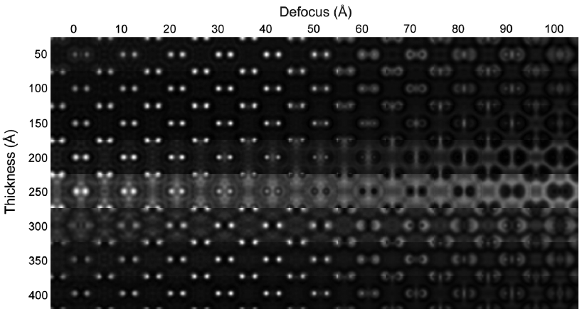
In particular, Urban and colleagues applied this new technique to a material where crystals can be grown with unmatched precision: silicon. The image below of silicon atoms clearly shows the “dumbbell” arrangement of silicon atoms in pairs.
The scattering patterns observed in these images are rather complex, and studying these and comparing them to computer models will make it possible to gain more information on the chemical elements in the samples. In this case, the sample consists of only one type of atoms – silicon. It will now be interesting to see how good this approach is in resolving different elements. Still, it is amazing to see how much progress still can be made with a relatively established imaging technique such as electron microscopy, and how new sciences arises from improved measurement techniques.
Note – 11 June 2013: this blog post has been corrected to state that FEI is an American company.

Mapping of silicon atoms in a high-resolution transmission electron microscope. The image shows a study of silicon atoms imaged for different microscope focus and sample thickness. Copyright (2013) by The American Physical Society.
Reference:
Urban, K., Mayer, J., Jinschek, J., Neish, M., Lugg, N., & Allen, L. (2013). Achromatic Elemental Mapping Beyond the Nanoscale in the Transmission Electron Microscope Physical Review Letters, 110 (18) DOI: 10.1103/PhysRevLett.110.185507


June 11, 2013 at 15:23
This is an exciting time in electron microscopy since the resolution limit seems to have been overcome. Or at least the resolution limits of what is matter have been reached since what is there below 0.5 A with out have to delve into the realm of particle physics? With this limit removed experiments in the TEM can now move towards measuring dynamical properties in-situ as opposed to just trying to see what the sample is.
That said FEI is an American company, who has major development and manufacturing site in the Netherlands. Sorry to be pedantic, but the other half of the company designs and builds the instruments that make samples for these wonderful electron microscopes.
June 11, 2013 at 16:24
thanks for pointing this out Josh! I’ve corrected the error in the blog post.
June 12, 2013 at 17:49
Hi Jeorg no problem, I hate to get nationalistic, but for my former colleagues it can be a touchy issue, though I think on one level I am not sure nationality really matters for a big multi-national company.
anyways, back to microscopy…