Understanding the properties of something chaotic such as a bowl of spaghetti may seem a daunting task. But that’s what Garry Rumbles from the National Renewable Energy Laboratory in the USA, Natalie Stingelin from Imperial College London in the UK, and coworkers are trying to do. With success. They study polymers – long spaghetti-like molecules made of repeating atomic subunits – and have now uncovered how the microstructure of these polymers controls the behaviour of optically generated electrical charges in such a tangled molecular web, with important implications for the design of electronic devices.
The physical properties of polymers depend a lot on the length of the molecules as a whole, the atomic make-up of their structural units and the physical interactions between the individual strings. That’s why polymers come in so many forms, from hard plastics to stretchable synthetic rubbers. And what Stingelin and Rumbles now show is that also their electronic properties depend not only the chemical make-up of the polymers, but also the details of their structure and their molecular weight. This has dramatic consequences for the search of new polymers for various optical and electronic applications, says Stingelin. “Are there otherwise wonderful polymers out there that were cast aside because their creators tested the wrong molecular weight? We think it’s quite possible.”
[…]
Continue reading...

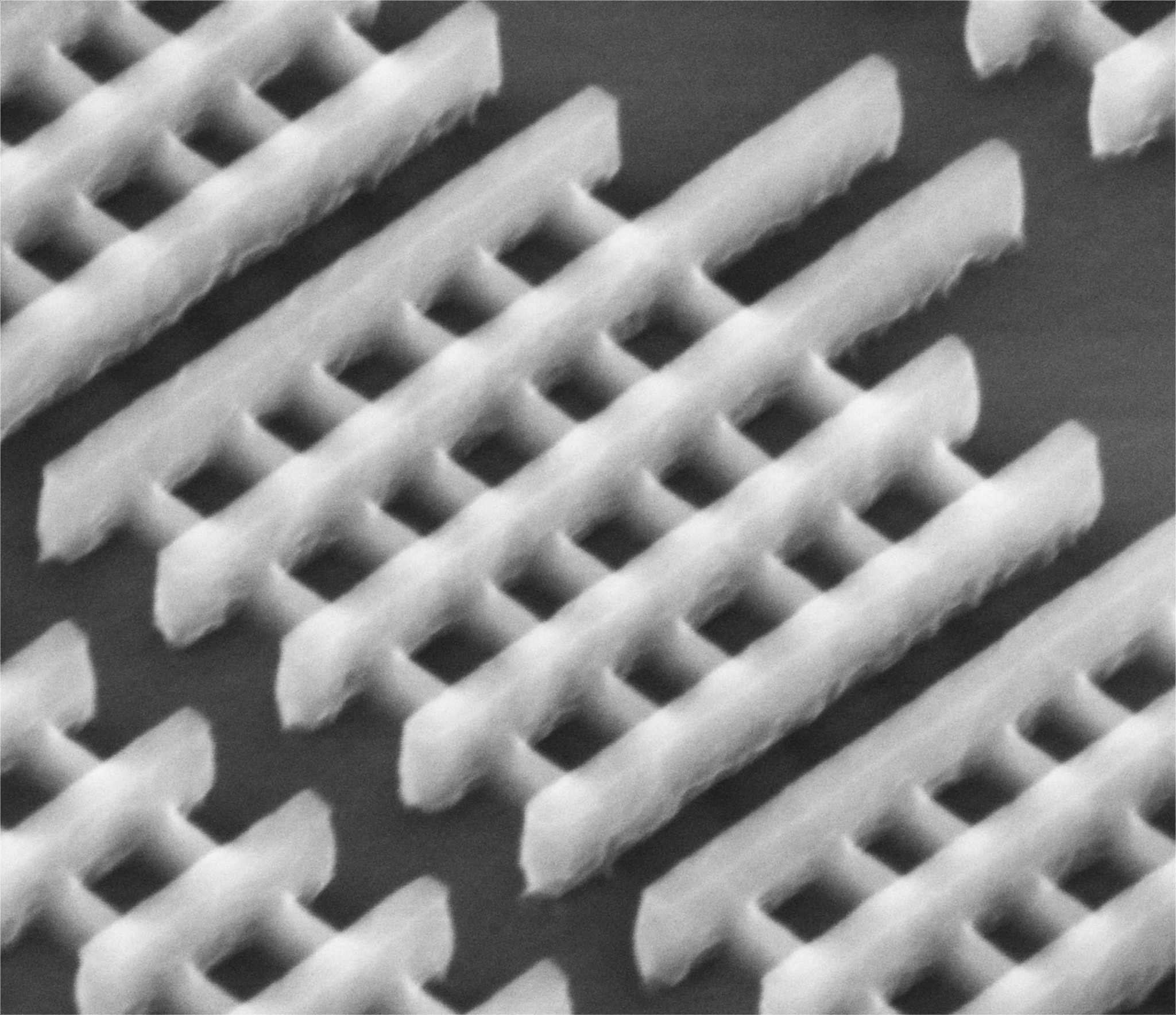
Intel's 3D tri-gate transistors have a feature size of only 22 nm. The thin structures are the silicon channels, the thicker ones are the gates and the contacts. Several gates can be used next to each other to enhance the efficiency of the switching. (c) Intel
Finally I am getting around to blog about the latest generation of transistors that Intel presented earlier this months. These transistors reach feature sizes of only 22 nanometres, down from 32 nm. To give you some perspective what this amazingly high integration means: 4,000 of those 22 nm structures fit across the width of a human hair, or similarly, 100 million of these transistors fit on the head of a pin.
Now how did they reduce transistor length scales down by almost a third? Well, even though Intel (and others) is in the business of shrinking transistor for more than 40 years, this time it’s a bit more than a mere scaling exercise. For the first time we have a commercial 3D transistor design on such a scale. In a typical ‘field-effect’ transistor, two electrical contacts are used to run an electric current through a silicon layer. The transistor is switched between an electrically conducting and an insulating state by a gate on top of the silicon. The voltage applied to that gate determines whether current can flow or not. Thereby the gate is able to set the digital ‘1’ and ‘0’ in a transistor.
A problem in shrinking transistors has been the fact that those three electric contacts need a certain minimum space of their own. Furthermore, as the gate has become smaller and smaller, it has been increasingly inefficient to switch the electric current in the silicon layer underneath. For smaller gates the electric fields from the gate just don’t reach that far down into the silicon layer. […]
Continue reading...
Fibre optic cables transmit information so fast because they can make use of the unique properties of light and transmit many data channels at the same time. The digital 1s and 0s the light beams carry are imprinted onto the beams by semiconductors that in quick succession turn the light beam on and off. Unfortunately, that also puts a limit on the possible data rate, as materials switch slower than light. There are all-optical switches operating at the speed of light using special crystals, but what is needed are solutions that can be fabricated on a chip.
This is made possible now. Georgios Ctistis, Willem Vos, Jean-Michel Gérard and colleagues from the University of Twente and the FOM-Institute Amolf in the Netherlands, and the Institute for Nanoscience and Cryogenics in Grenoble in France have demonstrated that using a material to switch light is not a drawback anymore. They are able to switch a light beam within a semiconductor device at speeds of 0.3 picoseconds, where a picosecond is a millionth of a millionth second. That’s so fast that it approaches the limit set by the speed of light.

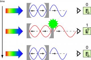
The principle of the ultimate optical switch. Top: a microcavity blocks the transmission of the red signal beam. Middle: in the presence of a control beam the cavity changes its properties and lets the beam pass. Bottom: as the control beam is off again, the switch also turns off. Figure provided by the authors.
In a conventional optical switch, a light beam (or an electrical voltage), is used to excite electrons in a semiconductor. These electrons then change the material’s optical properties in a way that switches the signal beam on or off. But this is a comparatively slow process. The idea here is to separate the optical effects from materials properties, which would only slow the device down. “The key advance is that both the switch-on and -off times of the semiconductor microcavity is completely determined by the properties of light itself,” says Vos.
[…]
Continue reading...


October 18, 2011
1 Comment