Archive | Materials Science RSS feed for this archive

Graphene and the innovation gap

December 8, 2013

3 Comments

This week some rather pessimistic articles on graphene’s commercial potential appeared in the UK press. On Tuesday, Aditya Chakrabortty commented in the Guardian on “How UK wonder substance graphene can’t and won’t benefit UK“, highlighting some pretty poor statistics when it comes to the innovation in graphene here in the UK, where Andrei Geim and Kostya Novoselov carried out their pioneering research:

Our record with graphene has been similarly dismal. Consultants calculate that China has taken out more than 2,200 patents on the material; the US more than 1,700; South Korea is closing in on 1,200. And the country that discovered it? Just over 50.

One of the problems, Geim is quoted in the article, is that there isn’t industrial sponsorship for his research:

Here is one of the world’s great scientists, pointing out that British businesses are either incapable or unwilling to use his inventions. The effect is rather like James Watt complaining that he can’t find any takers for his new steam engine.

This negative picture from a research perspective has been contrasted from the industrial side with a commentary by Jonathan Ely in the Financial Times this Saturday, saying there is too much investment into graphene: “The growing graphene investment bubble” (reading this link requires free registration at the FT). For Ely it seems the problem is not the industrial side – several companies now are on the market aiming to commercialize graphene – but that there is just nothing interesting about graphene (even though the Guardian continues to call it a ‘wonder’ material):

Graphene has been around since 2004, and many patents connected with it have been filed around the world (the Koreans are especially interested). Bill Gates has suggested it be used to make indestructible condoms to prevent the spread of disease in the developing world. But so far there are no widespread commercial uses for it.

How to consolidate these contrasting views? Perhaps the problem is that companies do not see the potential of graphene in the same way as Geim does. Graphene came from blue sky innovative research done by Geim and Novoselov, born more out of curiosity than because of commercial aspirations. Still, when the Nobel prize was awarded to these pioneers, commercial applications featured prominently in the comments of the Nobel Prize committee. This even caused me to call for caution on the technological potential. And it is fair to say that the promised broad-sweeping applications particularly based on graphene’s electronic properties have not yet materialized.

But this does not mean that all is bleak. […]

Continue reading...

X-ray crystallography made easy

April 1, 2013

1 Comment

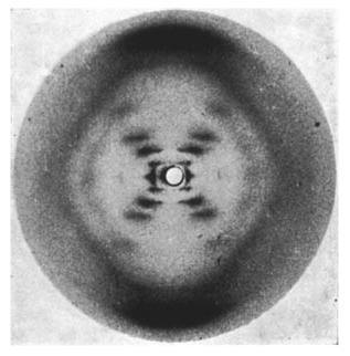
Sixty years ago this month Nature published the famous paper by Watson and Crick solving the structure of DNA. At the time many researchers pursued this goal, made difficult by the complexity of the DNA itself. A key contribution to the solution of the puzzle was the x-ray diffraction data provided by Rosalind Franklin. Indeed, without x-ray diffraction experiments this discovery would have been almost impossible at the time.

X-ray diffraction image of DNA. (c) Nature Magazine. Franklin, R. & Gosling, R. G. Nature 171, 740-741 (1953) - doi:10.1038/171740a0

Rosalind Franklin’s x-ray diffraction image of DNA. (c) Nature Magazine. Franklin, R. & Gosling, R. G. Nature 171, 740-741 (1953) – doi:10.1038/171740a0

The way x-ray crystallography works is that a beam of x-rays is directed at a crystal, where the x-rays bounce off the atoms. Because the atoms in a crystal are periodically arranged, the x-rays form complex but regular patterns (such as the one seen for DNA). A detailed analysis of these patterns enables the precise determination of the crystal structure.

To this day such experiments aren’t easy. They require relatively large crystals and typically are done at major facilities such as electron synchrotrons. The synthesis of the crystals for these experiments can often be very difficult.

Yasuhide Inokuma, Makoto Fujita and colleagues from the University of Tokyo in Japan  and the University of Jyväskylä in Finland have now developed a clever method that does away with many limitations of x-ray crystallography. Their method works with tiny amounts of material, only about a half to 5 micrograms are enough. This is around a millionth of a gram – truly tiny. The difference between a microgram and a gram is the same as that between a gram and a metric ton. In addition, another major advance of their method is that the target molecules don’t even need to be in a crystalline state. […]

Continue reading...

Samarium hexaboride

December 12, 2012

1 Comment

There is a lot of buzz in the physics community about a new topological insulator: samarium hexaboride, SmB6. The reason why any major discovery about topological insulators seems to be big news is that these materials have some unique electrical characteristics that make them not only very interesting from a fundamental point of view but also for electronic applications.

Topological insulators are electrically insulating in their interior, but at the surface they do conduct current. Moreover, the surface currents are topologically protected (hence the name), which means that the electrons that carry those currents don’t veer off the track easily and maintain their properties over long distance. Although a number of topological insulator compounds are known, the problem so far has been that it has been difficult to fabricate these with sufficient purity such that the interior was indeed insulating. This has been a problem, as the electrical current inside the materials just overwhelms the surface properties. […]

Continue reading...