Archive | Materials Science RSS feed for this archive

Yet more graphene transistors – it’s twins!

September 8, 2010

1 Comment

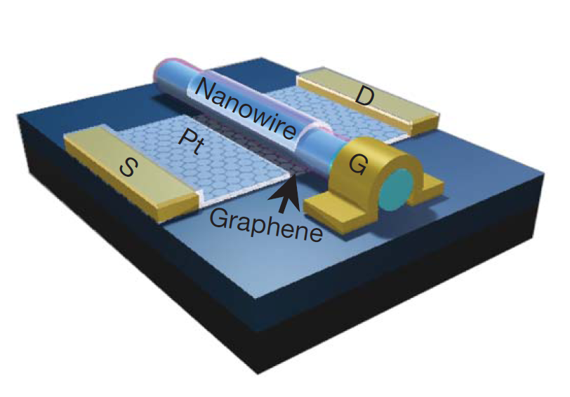
Last week I blogged about a Nature paper on graphene transistors with a self-aligned nanowire gate.  Well, as I gather from a blog post by Doug Natelson, largely the same UCLA researchers have now published a paper in Nano Letters that uses a rather similar idea, even though in the latest paper the nanowire gate is made from another material, and it seems the latest transistors are even faster.

However, I am worried about the obviously parallel publication of these two papers. The Nature paper was submitted 23 May, published 1 September. The Nano Letters paper was submitted 16 May and published 3 September.

As Doug says: “Looks like they managed to get two papers in good journals for the price of one technique advance.” And I agree, it looks very much like salami slicing of research results to me. In particular, I like to emphasize that it is editorial policy of Nature journals that editors (like myself) are informed about any related submission made to other journals — see Nature‘s policy on duplicate submissions and plagiarism.

I have not checked this fact with my colleagues and if I would have I could not comment here on my private blog, but I do wonder whether such communication has taken place here. If I were the handling editor, this dual publication would not have been knowingly possible, but others might of course have a different opinion.

Either way, in cases where our policy on duplicate submission is not followed, little can be done if clearly different materials were used, even if a study is based on a similar concept. Apart from increased scrutiny of such authors in future submissions of course.

References:

Liao, L., Bai, J., Cheng, R., Lin, Y., Jiang, S., Qu, Y., Huang, Y., & Duan, X. (2010). Sub-100 nm Channel Length Graphene Transistors Nano Letters DOI: 10.1021/nl101724k

Liao, L., Lin, Y., Bao, M., Cheng, R., Bai, J., Liu, Y., Qu, Y., Wang, K., Huang, Y., & Duan, X. (2010). High-speed graphene transistors with a self-aligned nanowire gate Nature DOI: 10.1038/nature09405

Continue reading...

The thing with graphene transistors

September 1, 2010

6 Comments

Graphene is one of the hottest research areas in nanotechnology, and it may seem slightly surprising it took me a month to write my first blog post on the topic. That moment has now come, with the advance publication of a Nature paper that presents highly attractive graphene transistor, even though in my humble opinion the approach taken seems not the most promising for future highly integrated devices.

There are many reasons why graphene gets researchers so excited. The stability of this single layer of carbon atoms is one of the reasons, promising tough composite materials with increased mechanical strength. The unusual electronic properties that in some respect resemble that of relativistic particles is another. And last but not least, the fact that electrons can travel ballistic, without hitting carbon atoms, for long distances in the micrometer range is another. All these contribute to graphene’s success.

Schematic of the device where a nanowire acts as gate for a graphene transistor. Reprinted by permission from Macmillan Publishers Ltd. Nature (2010). doi:10.1038/nature09405

Two years ago I wrote a feature in New Scientist where I focussed on the potential of graphene to replace silicon logic. The piece is now behind a pay wall, but when talking to Andre Geim at the time, a pioneer in the field, he told me that graphene is uniquely suited to scale down to device dimensions impossible to achieve with silicon. Any transistor needs to support an electric current, that is how you read out its status. However, if you shrink the size of a transistor to only a few nanometers, this electric current will flow across only a small number of atomic bonds. Silicon bonds might not be able to sustain such high current densities. Not so graphene. “The bonds between the carbon atoms in graphene are very strong and can carry exceptionally high currents,” said Geim back then.

[…]

Continue reading...

Solar cells brought into shape

August 31, 2010

8 Comments

Photo by Scott Robinson (Clearly Ambiguous) via flickr.

Solar energy is a huge market and any improvement to the efficiency of solar cells has a significant impact. In 2008, worldwide photovoltaic solar energy production was about 5 gigawatts, and this is expected to rise to 15 gigawatts in 2015. To put this figure in context, a nuclear reactor produces around 1 to 1.5 gigawatts of electricity.

The overall conversion efficiency of the best solar cell devices, with complex designs that include multiple materials, reaches up to about 50%. For more common silicon-based solar cells efficiencies are around 20%, although commercial photovoltaic panels achieve even less than that. Any enhancement in solar cell efficiency, whether it is in terms of costs or in terms of efficiency, is therefore highly desirable and significant. If all photovoltaic cells that produce those 5 gigawatts of energy were only 5% more efficient, for example with 21% conversion efficiency instead of 20%, it would result in an increase in energy production equivalent to about 250 megawatts.

Another issue is cost. Bulk solar cells are better at catching more sunlight, but use more material and therefore cost a lot more than thin-film films. Albert Polman, Harry Atwater and colleagues have now developed a solar cell design that enhances the power efficiency of thin solar cells. In their study published in Optics Express they are able to enhance the efficiency of a 340 nanometer thick silicon solar cell by 27% when compared to a regular thin-film cell.

[…]

Continue reading...