Archive | Materials Science RSS feed for this archive

Glasses tougher than steel

January 9, 2011

8 Comments

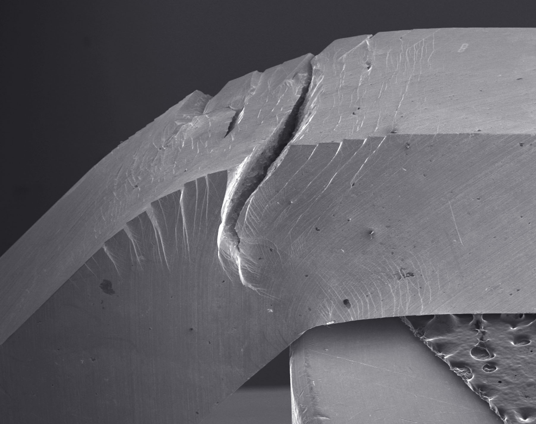
A tough metallic glass. This Pd79Ag3.5P6Si9.5Ge2 glass did not fracture catastrophically even after undergoing significant bending. Credit: Maximilien E. Launey

Glasses are very useful structural materials, because they are strong. You can stand on a glass table without it breaking. But once you put too much stress on a glass it breaks. Steels on the other hand are much tougher — which means that they show a much stronger resistance to fracture: rather than suddenly breaking under stress, steels tend to deform first. This toughness of steel is one of the obvious reasons why steel skeletons instead of glasses are used for the construction of large buildings.

This conception of glasses not being very tough is now made history by Marios Demetriou and colleagues from the California Institute of Technology and The University of California, Berkeley. They have discovered a glass that is not only strong, but also tough as steel. It is a metallic glass, which means that it dominantly consists of metal atoms. Like other metallic glasses it isn’t transparent, but looks like a normal metal  — except that unlike crystalline metals its atomic structure is more or less random. The damage tolerance of this metallic glass, its combination of strength and toughness, is higher than any known material. “It has been usual to regard metallic glasses as damage sensitive, but over recent years it has become increasingly recognised that they can be tough. This new paper marks a further decisive shift in showing that metallic glasses can be very tough indeed,” says Lindsay Greer from Cambridge University, who studies the properties of metallic glasses.

[…]

Continue reading...

Catching up on nanophotonics

January 4, 2011

4 Comments

(c) Olympiaregion Seefeld

A key part of my job as an editor of a scientific journal is to attend to conferences. To scout new and exciting developments, to network with scientists, and to take a look at new research that I get shown in confidence. There is a lot to be gained by attending scientific meetings, and I am convinced that I couldn’t do my job as well without going to meetings.

This year, my conferences start early, I am presently attending the Nanometa conference, which coincidentally I helped to organise as a member of the technical programme committee. The conference takes place in the beautiful ski resort Seefeld in Austria.

Despite the beauty of Seefeld’s scenery, what attracted me to attend this conference is the topic — nanophotonics. Nanophotonics means the interaction of light with matter on extremely small length scales. Indeed, most nanophotonic devices are even smaller than the wavelength of light that they interact with. For example, the visible spectrum of light ranges from about 390 nanometers to about 800 nanometers wavelength, and these devices typically are on the same length scale or smaller — hence the name ‘nanophotonics’.

But what is the difference between nanophotonics and regular photonics? Well, conventional optical instruments, such as lenses, can only focus light down to length scales that are on the same scale as the wavelength of light. In the case of visible light this would be a few hundred nanometers. On the other hand, electronic devices such as transistors are smaller than that, on the order of tens of nanometers. So if you want to do photonics with say visible light on that kind of length scale, conventional optics simply won’t work.

One way to escape this dilemma is to use so-called surface plasmons, which are collective motions of electrons on the surface of a metal. These movements act like very powerful antennas that can create extremely strong light fields close to the surface of metal nanostructures. There are several exciting research trends based on such plasmonic devices that all are key parts of the conference here in Seefeld:

  • Plasmons can focus light very efficiently into solar cells: Because they are such strong antennas, gold nanostructures on top or at the back of a solar cell can very efficiently concentrate light into the device and that way enhance the efficiency of the light collection. This is of particular use for solar cells made of thin films, because if a solar cell is very thin, some of the light would simply pass through without getting absorbed. The intense light concentration by metallic nanostructures on the other hand counters exactly that. In comparison to thicker solar cells, such new devices won’t set world-records in efficiency, but they enable lighter solar cell modules that use less material. Therefore they promise to be more cost-efficient and resource-saving. For more information, see my earlier blog post ‘Solar cells brought into shape‘.
  • Plasmonic devices make efficient sensors: atoms and molecules absorb light at specific optical wavelengths that can be used to identify these molecules. The strong intensity of light around metal nanoparticles strongly amplifies the absorption, so that even a single molecule can be detected! Earlier last year I blogged about a clever way of doing that in ‘The dark side of photonics‘. There are also other ways of sensing, where the mere presence of a chemical molecule can alter the optical property of a nanophotonic device.
  • Plasmonic devices can transport light: An exciting talk at the conference was that of David Miller from Stanford University. He (and other scientists as well) highlighted the benefit of using light to transmit information on an electric chip. The currents between transistors on a computer chip produce a large amount of heat. So much heat in fact that shrinking transistors further and putting more of them on a chip can only work if this heat production is reduced. One way of reducing heat generation is to use optical beams instead of electrical conductors. And the best way to connect these tiny transistors optically is to use plasmonic metal nanostructures.
  • Last but not least, metamaterials for visible light use plasmons: metamaterials are devices that shape the propagation of light by being made from metallic structures that are smaller than the wavelength of light. This requires the use of plasmon effects. One of the most-quoted application of such metamaterials are invisibility cloaks, but there are plenty of others. In particular I like to re-emphasize my earlier comments on ‘What are the realistic promises of metamaterials and cloaking?

Obviously, this is only a small selection of the trends in the field. Many more developments emerging from this conference in Seefeld will appear in the scientific literature soon, and some of them will be covered on this blog for sure, simply because controlling light on such small length scales offers so many exciting opportunities!

Continue reading...

2010 – twelve months of great science

December 27, 2010

3 Comments

The past year has been a great year for science with major advances in several areas. Too many exciting results to mention here. Instead, to reflect about the past year I have chosen a representative paper for each month of the year that I hope can serve as an example of the great science going on in a number of research fields. Of course, this is a highly subjective and personal collection, and indeed there might be others worth mentioning. But the aim was also to provide a balanced overview of the year that covers a variety of topics.

Of course, if you have an exciting paper to add, please feel free to use the comments section below to let us know!

Anyway, enough said, here are some of my highlights from the past year:

Simulations of electronic excitations in an iron-based superconductor. Image by Oak Ridge National Laboratory via flickr.

JANUARY – iron-based superconductors

Since they were discovered in 2008, iron-based superconductors, the pnictides, have been one of the hottest topics in condensed matter physics. Part of their appeal stems from the fact that they are based on iron, which is a magnetic element. Normally, magnets and superconductivity exclude each other.

The iron-based compounds have a similar crystal structure as the so-called cuprates, which are the materials with the highest superconducting temperatures known. The mechanism for these high-temperature superconductors is unknown, and studying the iron-based superconductors may also be relevant to the understanding of the cuprates.

This paper published in Science shows for the first time that the electrons in the iron-based superconductors show a periodic arrangement that is different to the periodicity of the atoms in the crystal. Similar observations have been made in the cuprates, and their understanding is considered important to the mechanism of high-temperature superconductivity.

Chuang, T., Allan, M., Lee, J., Xie, Y., Ni, N., Bud’ko, S., Boebinger, G., Canfield, P., & Davis, J. (2010). Nematic Electronic Structure in the “Parent” State of the Iron-Based Superconductor Ca(Fe1-xCox)2As2 Science, 327 (5962), 181-184 DOI: 10.1126/science.1181083

[…]

Continue reading...