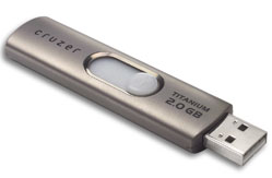
This USB flash drive used a bulk metallic glass for its casing. Credit: Liquidmetal Technologies.
This week I am attending the 2010 Materials Research Society Fall Meeting in Boston — one of the key meetings in materials science. One of the sessions is on bulk metallic glasses and their applications, which this year is a little special. It is organised in honour of the 50 year anniversary of the first demonstration of a metallic glass by William Klement, Ronald Willens and Pol Duwez from Caltech. Their paper on gold-silicon alloys was published in Nature on September 3rd, 1960. (In addition to Duwez and colleagues, David Turnbull must be mentioned here as one of the pioneers with several key contributions to the field. For example in 1948 he demonstrated that metals can be considerably undercooled below their crystallisation temperature.)
Metallic glasses have since become very interesting for applications that include sports products, coatings, power transformers where they reach several ten thousands of metric tons annual production, sports equipment, bioimplants and others. At the same time research researchers still try to learn more why these glasses form in the first place.
Why are metallic glasses so special?
All metals prefer to form crystals, as the metal atoms easily form structured bonds with other atoms. So easy in fact that even when the metal is melted some of that arrangement carries over into the liquid. This makes the formation of a crystal the preferred pathway once the melt is cooled down again. Glass on the other hand is amorphous, which means that the atoms are disordered and there is no long-range periodicity. This is not something metals prefer. Unlike the window glass made of silicon oxide. In comparison, metallic glasses are a very different animal. […]
Continue reading...
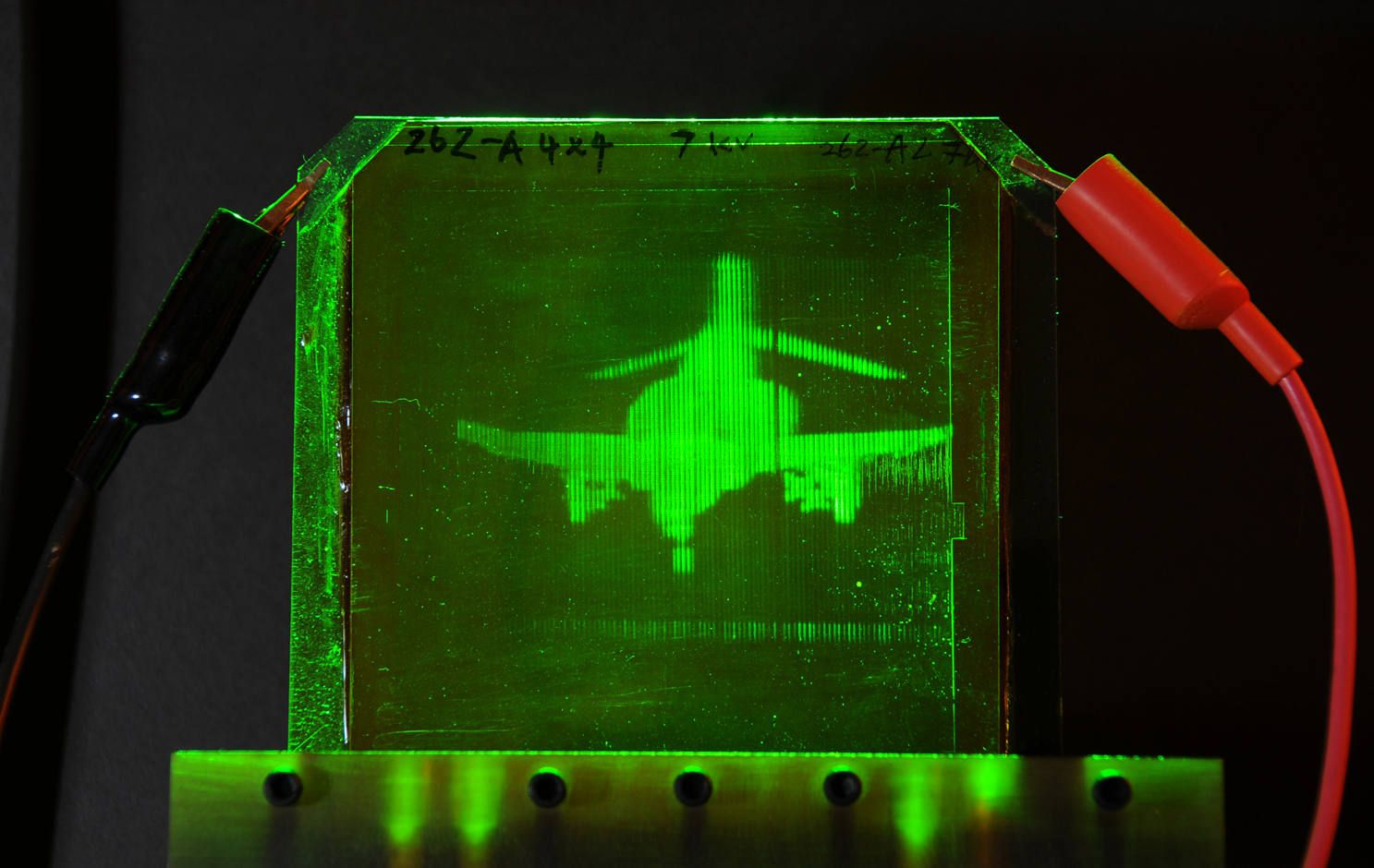
A refreshable holographic image of an F-4 fighter jet. Credit: gargaszphotos.com/College of Optical Sciences, The University of Arizona
Holograms may seem like an original invention from some science fiction films. A famous scene often mentioned in this context is that from Star Wars where Princess Leia records an important holographic message, ending with the words “Help me, Obi-Wan Kenobi“.
Such visions of holograms aren’t fiction. In a paper published in Nature, Nasser Peyghambarian, Pierre-Alexandre Blanche and colleagues from the College of Optical Sciences at The University of Arizona demonstrate a holographic system that is capable of displaying holograms at speeds approaching almost that of video capability. (and sure enough, they do mention Star Wars in the abstract of the paper…)
Holograms have been invented in 1947 by Dennis Gabor. They are made by shining a laser beam on an object and then recording the laser light reflected by the object on a photographic film. Simultaneously, a reference beam of the same laser is directly guided to the photographic film, where it causes an interference of the two beams. The interference pattern stored in the photographic film not only contains information on the light intensity (as in conventional photos) but also the phase difference between the two laser beams. The phase difference is a measure of the three-dimensional shape of the object. Together, intensity and phase contain the complete information of a light beam.
To recover the holographic image, the original laser needs to be used. Therefore, more practical ways of writing holograms have been develop and that do not require the original laser for viewing. Regular white light can be used instead. Although image quality for these holograms is not as good, they are widely used, for example on credit cards. Holograms can also be artificially created, without the use of an actual object, but by using a computer to calculate the necessary holographic interference pattern. Or information from a camera is digitally scanned and used to create a hologram elsewhere. “Holographic telepresence means we can record a three-dimensional image in one location and show it in another location, in real-time, anywhere in the world,” says Peyghambarian.
[…]
Continue reading...
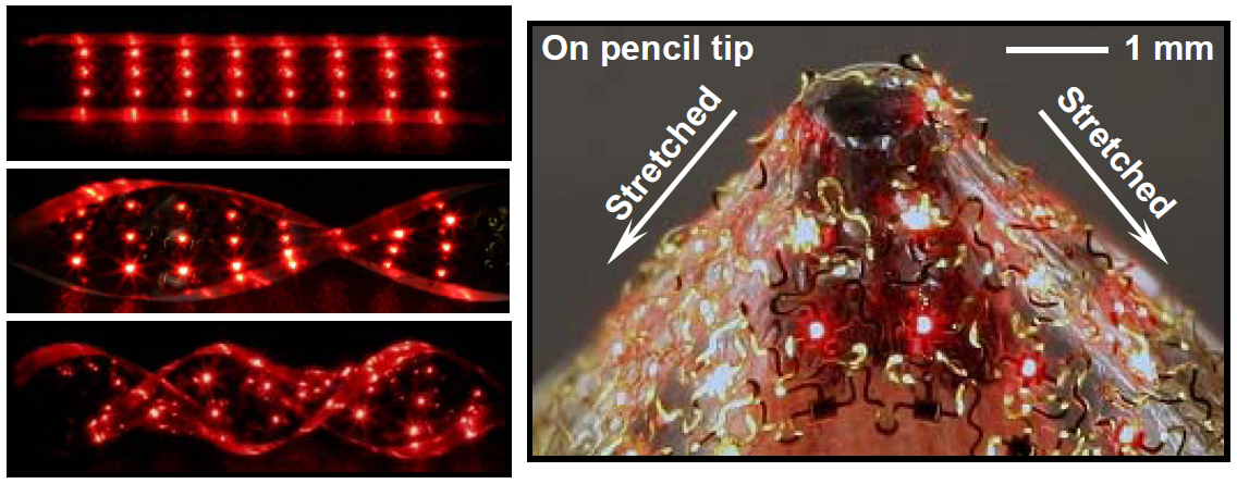
Stretchable electronic arrays. The LED sheets can be twisted by 720 degrees and considerably stretched. The wavy metal wires are visible in the image on the on the right. Reprinted by permission from Macmillan Publishers Ltd. Nature Materials (2010). doi:10.1038/nmat2879
Take a piece of silicon, try to bend it and it will break. Stretch a thin film of gold and it will rupture. Conventional metals and semiconductors are brittle and not elastic at all. But these are properties that you need when you want to use electronic devices in unusual places and for unusual applications. In biomedicine for example, if you want to put a diagnostic sensor on top of a muscle. In electronics, when you want to put a large-scale solar cell on the curved top surface of a car.
Sure, you can make a thin film and warp it around a cylinder, and if you do this with electronic circuits it is called flexible electronics. Organic electronics and very thin metal films on plastic can do this. But you cannot fit a two-dimensional sheet on a sphere without stretching it. For such applications you need what is called stretchable electronics, which is different to the flexible electronics that has been around for a while.
The latest milestone has been achieved by John Rogers and colleagues from the University of Illinois in Urbana-Champaign. They demonstrate (disclaimer: in my journal, Nature Materials) a fully biocompatible and implantable stretchable structure containing large arrays of light-emitting diodes and photodetectors. The sheets are stretchable and can be twisted by more than 720 degrees without damage, and can be brought into almost any desirable shape or configuration, says Rogers. “This advance suggests a technology that can complement features available with organic light emitting diodes, where peak brightness and lifetime are limited, and conventional inorganic LEDs, where relatively thick, brittle supports restrict the way that they can be integrated together and the substrates that can be used.”
[…]
Continue reading...


November 30, 2010
3 Comments