Archive | Materials Science RSS feed for this archive

Redoubled efforts in solar cells

October 4, 2010

5 Comments

Solar energy is obviously one of the key renewable energy resources available to us. At the same time researchers are hitting against a glass ceiling. A famous 1961 paper by William Shockley (who co-invented the transistor) and Hans Queisser comes to the conclusion that for a semiconductor such as silicon the maximum conversion efficiency of solar energy into electricity will never be more than about 30%.
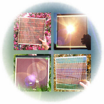
Dye-sensitized solar cells. A design similar to these solar cells is now used to demonstrate the creation and extraction of multiple charge carriers per photons.

One reason for this limit is that each light particle only excites one electron. Even if the electron has enough energy to excite two electrons, all this energy is lost and only one electron is excited. And this is the case for pretty much all present commercial solar cell technology. Fortunately, however, there are possible exceptions. Bruce Parkinson and colleagues from the University of Wyoming in the USA have now built a photovoltaic cell that at certain wavelengths of light can generate more than one electron per photon of light. Their approach promises to beat the Shockley-Queisser limit and could lead to solar cells with considerably enhanced efficiency.

In silicon and other semiconductors, if a photon excites an electron all excess energy is predominantly lost as heat. Of course, there are attempts to harvest the heat generated in solar cells, and such approaches could beat the Shockley-Queisser limit. And so could nanostructured materials that use for example plasmonic effects. But a more direct solution would be if the excess energy could be used to excite more than one electron in the first place.

[…]

Continue reading...

The very fabric of research: a visit to the ILL in Grenoble

September 20, 2010

3 Comments

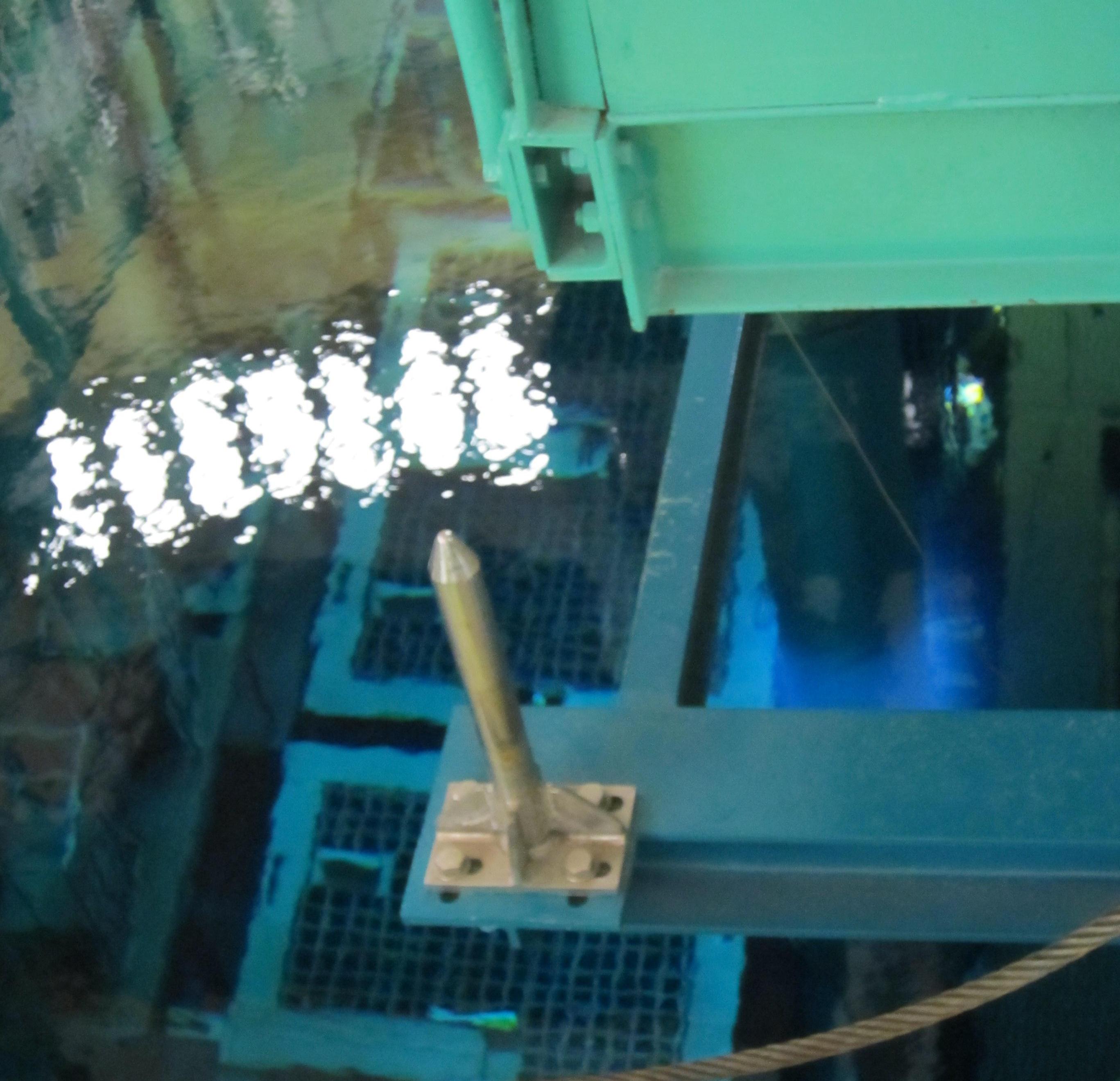
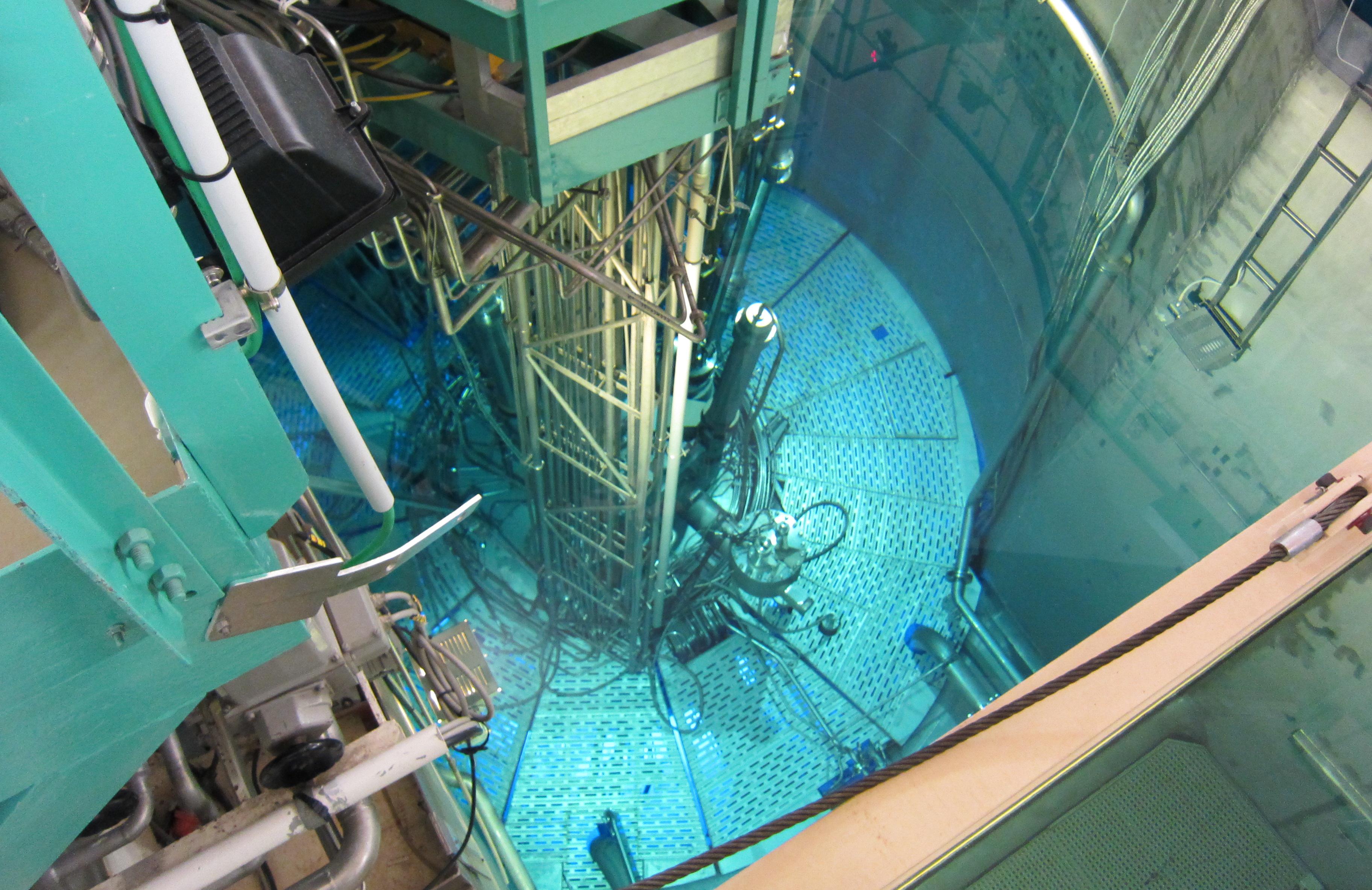
The nuclear reactor at ILL. The nuclear fuel is underneath the steel shield. The blue glow of that is partly visible is caused by Cerenkov radiation.

You look down into a clear pool of water. The water has an appealing blue glow to it that makes you want to dive into it. But this isn’t a swimming pool, it is a nuclear reactor. And the soothing blue glow is not due to the blue paint of the pool walls but caused by the Cerenkov radiation, emitted as a result of the electrons created by the fission process that move faster than the speed of light in water.

The electrons that are ejected from the nuclear fuel elements are fast than the speed of light in water (about 75% of the speed of light in vacuum). Similar to the supersonic bang of jets that fly faster than the speed of sound, Cerenkov radiation is emitted by water as the fast electrons pass through it. The blue shimmer of the Cerenkov radiation is visible on the right of the photo, showing the pool containing spent reactor fuel.

The reactor I am visiting is that at the Institut Laue-Languevin (ILL) in Grenoble. As a research reactor it is generating up to 58 megawatts of power, about 25 times less than that of commercial reactors. Still, I am nervous holding my camera directly above the pool to take pictures, afraid I might be dropping it into the running reactor. But there is no need to worry, it is safe to stand there, the water is a perfect shield from the radiation, it absorbs all the neutrons and electrons created by the nuclear reaction. And there is of course plenty of security and radiation monitoring before, during and after my visit. Even if I would drop the camera into the pool, there is a steel construction in the water that would catch larger objects. And stuff that would slip through that grid would probably lie harmlessly at the bottom of the pool until the reactor is decommissioned.

Not many people are allowed inside the reactor and I am lucky enough to be invited to the ILL along with a few British colleagues. It is only the second time I am inside a nuclear reactor. It is an awesome feeling, certainly for a physicist, to see an operating reactor and to admire the technology that keeps the nuclear chain reaction under control. The impressions from my visit not only reinforce what I know about the benefits of neutron research, but the variety of research to me also underlines the dangerous implications of possible recession-related government budget cuts to facilities like ILL.

ILL was founded by France and Germany in 1967, with the UK becoming a third major partner in 1973. Initially, the UK did not join the institute because it wanted to build its own reactor, tells us our tour guide, Andrew Harrison, an Associate Director of ILL. Nowadays it seems almost unbelievable to me that the UK abstains from a European research project because it intends to invest more money into a certain area of research, not less. In any case, today, Germany, France, and the UK still share 75% of ILL’s operating budget of 88 million Euros, the rest being distributed amongst its other international partners. Their continuing support has made ILL one of the leading research institutions that uses neutrons for experiments in life sciences (18% share of experiments), environment (11%), materials science (29%) and fundamental sciences (35%).

[…]

Continue reading...

In other news: you can even feel the goosebumps

September 14, 2010

1 Comment

Flexible electronics has been promising a lot for a long time. Organics-based electronics on our clothes and other wonderful gadgets. However, the real potential of the truly bendy stuff hasn’t been compellingly demonstrated for a long time. Sure, you can make wires on a plastic substrate and hope for the best. Which often wasn’t very much in terms of durability and bendability. The situation has only changed in the past four or five years, as nanotechnology devices have been  incorporated onto flexible polymer substrates.

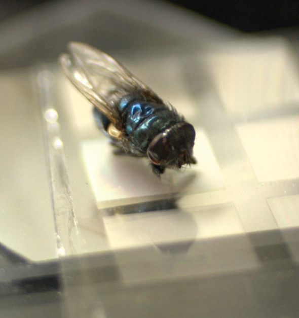
The weight of a fly is sufficient to trigger a signal in the artificial skin pressure sensor realized by Zhenano Bao and colleagues.

The weight of a fly is sufficient to trigger a signal in the artificial skin pressure sensor realized by Zhenano Bao and colleagues. The white PDMS units are visible underneath the fly. Reprinted by permission from Macmillan Publishers Ltd. Nature Materials, advance online publication (2010)

A good example of how far flexible electronics has come are two papers that have just been published in Nature Materials (note: I did not handle either of them as an editor). Both studies realize an “artificial skin” consisting of an array of sensors for position-resolved detection of pressure. As I suspected, both studies received plenty of press coverage, see the articles on Nature News and the BBC website. So here just a few salient points on both of them.

In one of the papers, Ali Javey and colleagues from Berkely use a grid of nanowire transitors to read out signals from a pressure-sensitive rubber membrane. The other study by Stanford’s Zhenan Bao uses PDMS as a pressure-sensitive element that changes its capacity on application of pressure. This information is read out with organic transistors. In the present realisation, Bao’s devices are attached to a silicon substrate, which limits their flexibility.

While for this reason Javey’s arrays are more flexible, with bending radii of 2.5 mm, Bao’s sensors excel with their pressure sensitivity of only 3 Pa. Atmospheric pressure is 101,325 Pa.

The different strategies employed by both groups show the versatility of the field, and the possibility to tailor material properties according to very specific requirements, whether conformability is desired, or sensitivity.

In many news articles on both papers there was a lot of talk about the use of these structures in “artificial skins”. Well, I’d say before we can think in earnest about such uses, there are plenty of practical problems to solve in terms of scalability, durability, stretchability, conformability and so on. At this stage, in my opinion, the flexibility and the sensitivity achieved with these technologies is already exciting enough to give you goosebumps — a sensation that probably could be resolved by the high-sensitivity sensors if they touched your skin.

References:
Mannsfeld, S., Tee, B., Stoltenberg, R., Chen, C., Barman, S., Muir, B., Sokolov, A., Reese, C., & Bao, Z. (2010). Highly sensitive flexible pressure sensors with microstructured rubber dielectric layers Nature Materials DOI: 10.1038/NMAT2834

Takei, K., Takahashi, T., Ho, J., Ko, H., Gillies, A., Leu, P., Fearing, R., & Javey, A. (2010). Nanowire active-matrix circuitry for low-voltage macroscale artificial skin Nature Materials DOI: 10.1038/NMAT2835

Continue reading...