Move over graphene, there is competition in town. A new type of two-dimensional materials – with the far less appealing family name, transition metal dichalcogenides – are increasingly gaining attention. Well, at least they’re giving it a shot. Graphene, a sheet of carbon atoms only one atomic layer thick, still has plenty going for itself in terms of electronic, optical and mechanical properties. There seems nothing that graphene can’t do.
On the other hand, there are also limits. When it comes to its electronic properties graphene is not a semiconductor in the same was as silicon is. It is lacking a bandgap, a gap in its electronic states that is important for light emitters and for some electronic devices.
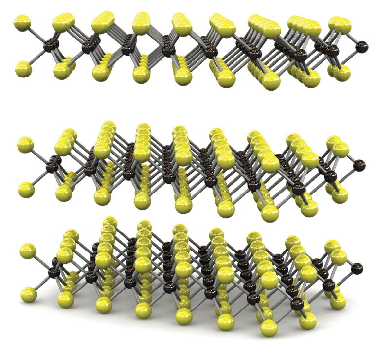
Schematic model of transition metal dichalcogenide atomic layers. The yellow balls represent the chalcogenide atoms, the blue ones the transition metals. Reprinted by permission from Macmillan Publishers Ltd. Nature Nanotechnology (2012). doi:10.1038/nnano.2012.193
Transition metal dichalcogenides offer an advantage there. They are semiconductors, and they can have a bandgap. And as their name says, they are formed by a combination of chalcogens such as sulphur or selenium and transition metals such as molybdenum or tungsten. Typical examples are MoS2 or MoSe2. These materials have become such hot stuff now that their properties have been reviewed in this month’s issue of Nature Nanotechnology. And even though the field is still young, there is plenty to review. […]
Continue reading...
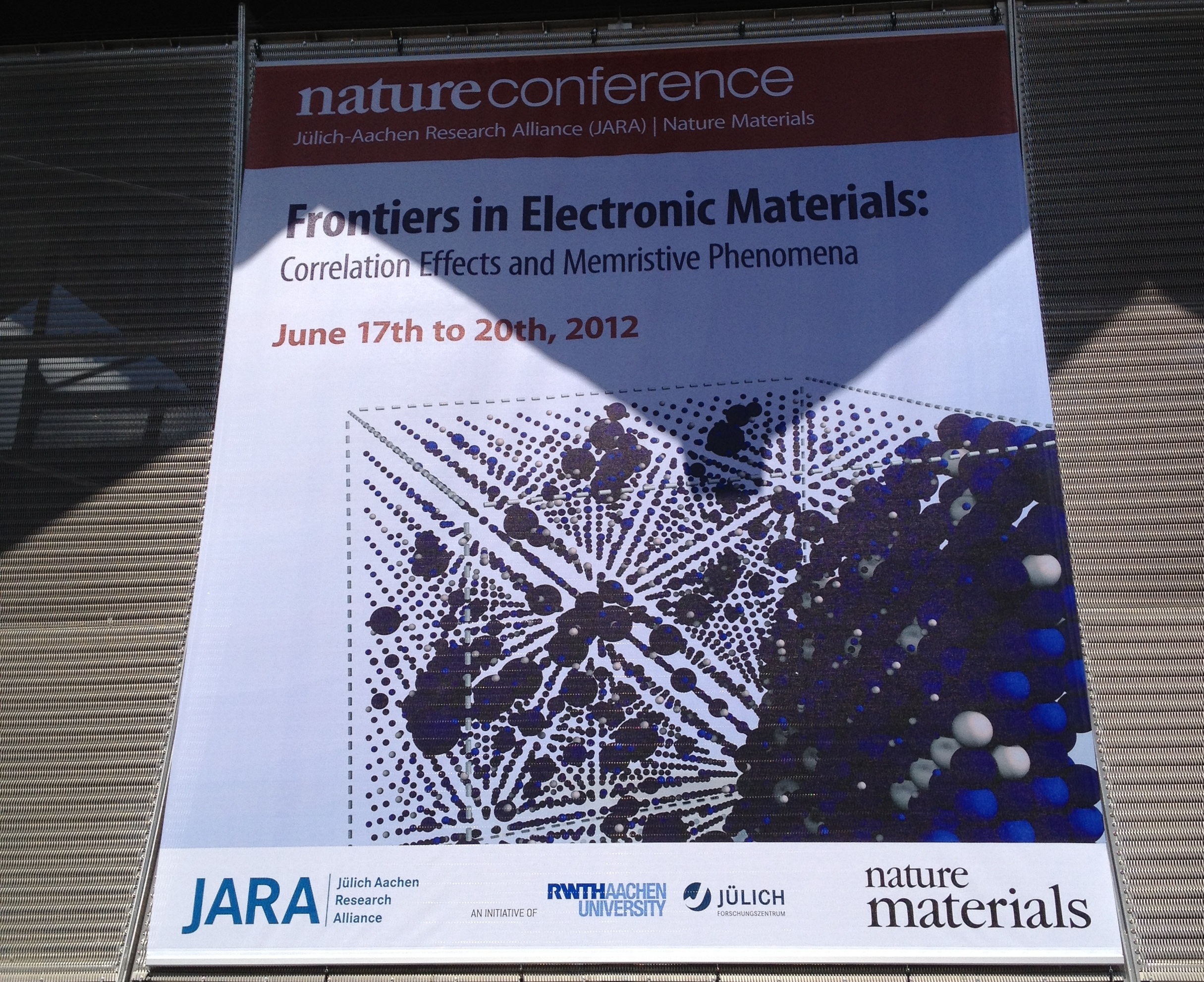 For the past weeks this blog has been more quiet than usual. Mostly, I was busy with a number of projects, including the co-organisation of a Nature Conference – ‘Frontiers in Electronic Materials: Correlation Effects and Memristive Phenomena‘. The conference took place in Aachen/Germany, and was organized in collaboration with the Jülich-Aachen Research Alliance (JARA) formed by the RWTH Aachen University and the Helmholtz research centre in Jülich – who did a great job in getting this meeting off the ground. Rainer Waser in particular dedicated a tremendous amount of work to the conference. And with close to 600 attendees, the popularity of the conference certainly exceeded all our expectations.
I do not intend to summarize all the interesting talks at the conference here. Instead, I like to focus on two aspects that I think contributed in particular to the success of the conference, and that could be of interest also to those that couldn’t attend the meeting. They’re related to the scope of the conference and its organisation. […]
Continue reading...
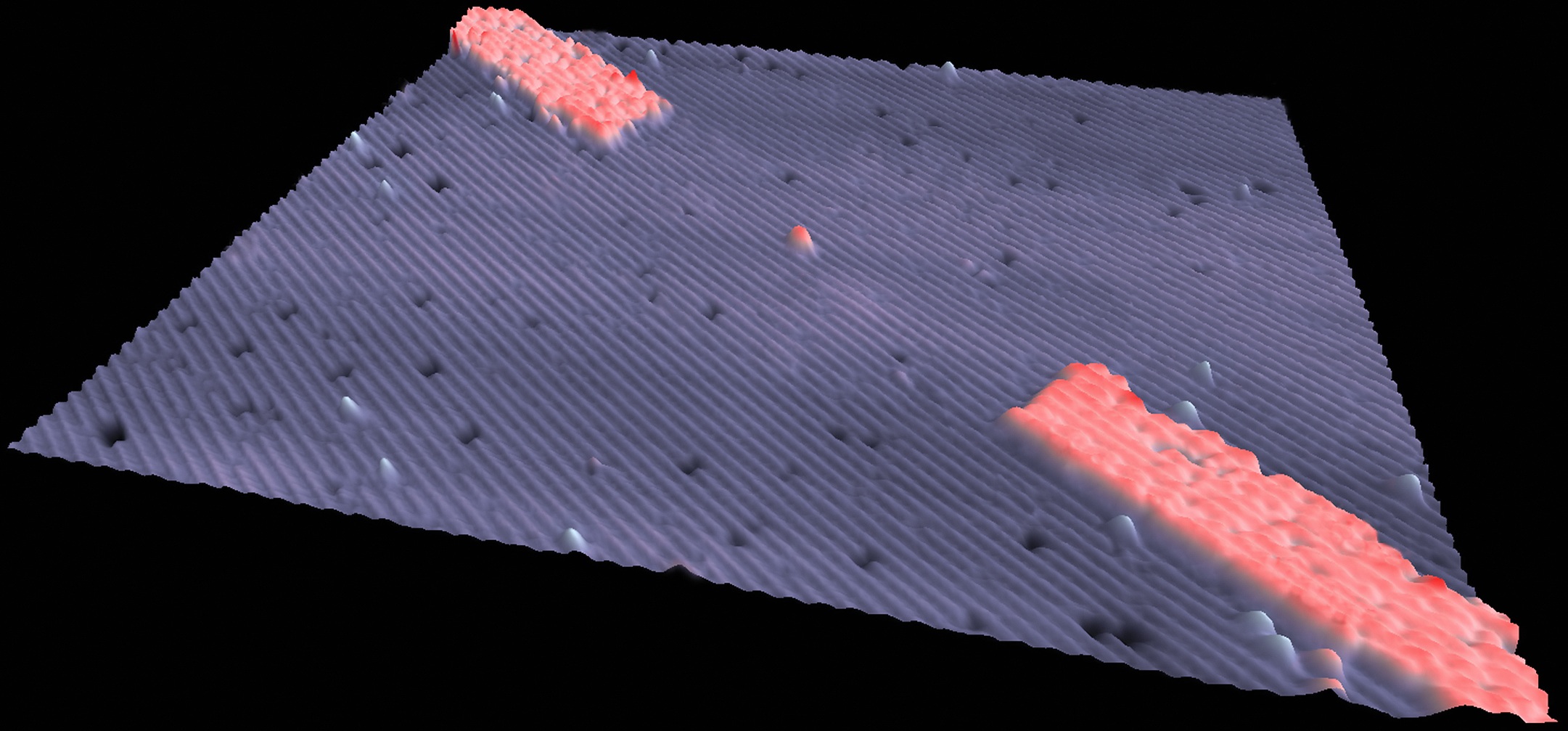
A scanning tunnelling microscope image of a single-atom transistor during fabrication. The pink colours represent the areas where a single phosphorus atom (centre) as well as phosphorus source and drain contacts will be placed. The gate contacts that control the transistor action from the side are not visible here. Credit: Martin Fuechsle
When Gordon Moore made his observation in 1965 that the number of transistors integrated on a single silicon chip is doubling roughly every two years, the only logical end point for such a trend would be a transistor made from a single atom. This point has now been reached. Writing in Nature Nanotechnology, Michelle Simmons from the University of New South Wales in Sydney and colleagues report a single-atom transistor, the world’s smallest, on a silicon chip. The transistor is based on current flowing through a single atom of phosphorus embedded in a silicon wafer. […]
Continue reading...


 For the past weeks this blog has been more quiet than usual. Mostly, I was busy with a number of projects, including the co-organisation of a

November 13, 2012
2 Comments