Symphonies are some of the most complex musical pieces. They involve different instruments, each with their own unique sound, and each instruments section playing their own tunes. Yet, what are symphonies in comparison to the complexity of life? Proteins for example, they are made of a limited number of building blocks, amino acids, but take highly complex shapes and assume a broad range of functions in the body.
Still, there is a commonality underlying such complex systems, in many cases they are hierarchical, which means they’re made of different objects on different scales – instruments playing tunes, amino acids forming proteins and so on. As David Spivak, Markus Buehler and others from MIT have described in a recent paper, a mathematical approach, known as category theory, can be used as a versatile tool that is capable of modelling complex systems by using the underlying rules governing a structure’s components. This is a very powerful approach and there is a lot to be gained by using this mechanism in materials science, to describe biomolecules or other hierarchical materials. Moreover, their approach makes it easy to connect different complex system. To put it crudely, understanding a Beethoven symphony may also provide insights into the properties of a protein, because category theory helps us links various complex systems.

Photo by Wayne Dixon via flickr.
To understand how this works, let’s take a look at an example provided by Buehler and colleagues – spider webs. These are made of individual fibres, consisting of smaller fibrils. The fibrils are made of a nanocomposite of crystal-like structures connected by flexible links. These structures are in turn made of various amino acids.
The complex structural hierarchy of spider silk (and other systems) is of course well-known. The problem researchers face is, however, that knowing the individual components of a material doesn’t necessarily mean that the properties of the full system are known. For example, even though the molecular composition of a protein may be known, predicting its three-dimensional shape is notoriously difficult. It is the behaviour of structural elements in the context of their use that can be so difficult to understand. And this is where category theory is useful. […]
Continue reading...

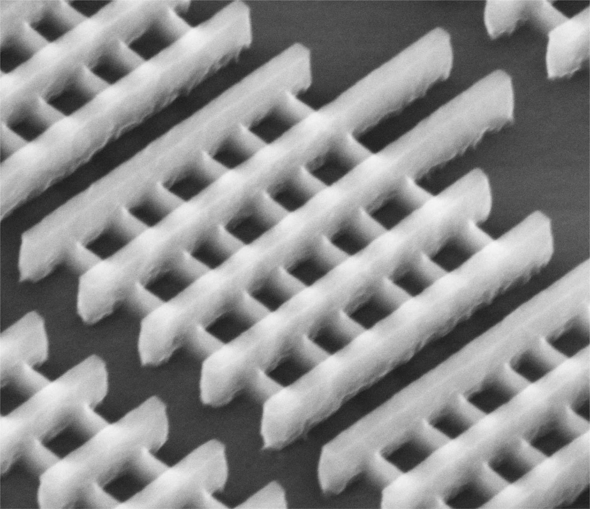
Intel's 3D tri-gate transistors have a feature size of only 22 nm. The thin structures are the silicon channels, the thicker ones are the gates and the contacts. Several gates can be used next to each other to enhance the efficiency of the switching. (c) Intel
Finally I am getting around to blog about the latest generation of transistors that Intel presented earlier this months. These transistors reach feature sizes of only 22 nanometres, down from 32 nm. To give you some perspective what this amazingly high integration means: 4,000 of those 22 nm structures fit across the width of a human hair, or similarly, 100 million of these transistors fit on the head of a pin.
Now how did they reduce transistor length scales down by almost a third? Well, even though Intel (and others) is in the business of shrinking transistor for more than 40 years, this time it’s a bit more than a mere scaling exercise. For the first time we have a commercial 3D transistor design on such a scale. In a typical ‘field-effect’ transistor, two electrical contacts are used to run an electric current through a silicon layer. The transistor is switched between an electrically conducting and an insulating state by a gate on top of the silicon. The voltage applied to that gate determines whether current can flow or not. Thereby the gate is able to set the digital ‘1’ and ‘0’ in a transistor.
A problem in shrinking transistors has been the fact that those three electric contacts need a certain minimum space of their own. Furthermore, as the gate has become smaller and smaller, it has been increasingly inefficient to switch the electric current in the silicon layer underneath. For smaller gates the electric fields from the gate just don’t reach that far down into the silicon layer. […]
Continue reading...

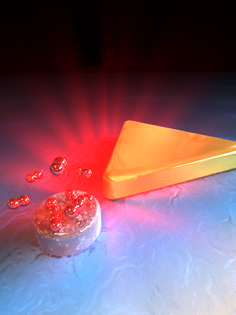
Hydrogen sensing at the nanoscale. Hydrogen molecules (red) are absorbed by a palladium nanoparticle (silver) and the resulting changes in optical properties amplified by a gold antenna. (c) Mario Hentschel, Na Liu, Harald Giessen
Sensing the presence of molecules in gases and liquids is a billion dollar business. Just think about all the carbon monoxide detectors in private homes, or blood glucose sensors. In particular for many technical and scientific applications, ultrasmall and precise sensors are desired. This includes sensors to measure gases in catalytic nanoreactors and fuel cells, or the monitoring of biochemical processes.
Laura Na Liu and Ming Tang from the group of Paul Alivisatos, director of Lawrence Berkeley Lab in the USA, and Mario Hentschel from Harald Giessen‘s group at the University of Stuttgart in Germany have now developed a new class of optical nanoscale sensors that are able to measure specific molecular concentrations down to single particles. This, says Alivisatos, “should pave the road for the optical observation of chemical reactions and catalytic activities in nanoreactors, and for local biosensing.” Their paper is published this week in Nature Materials (declaration of interest: I was the handling editor of this paper, although I like to stress that I don’t benefit in my day job by blogging about this work). […]
Continue reading...


December 12, 2011
Comments Off on The Beethoven connection