Archive | Nanotechnology RSS feed for this archive

2010 – twelve months of great science

December 27, 2010

3 Comments

The past year has been a great year for science with major advances in several areas. Too many exciting results to mention here. Instead, to reflect about the past year I have chosen a representative paper for each month of the year that I hope can serve as an example of the great science going on in a number of research fields. Of course, this is a highly subjective and personal collection, and indeed there might be others worth mentioning. But the aim was also to provide a balanced overview of the year that covers a variety of topics.

Of course, if you have an exciting paper to add, please feel free to use the comments section below to let us know!

Anyway, enough said, here are some of my highlights from the past year:
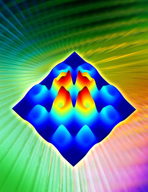
Simulations of electronic excitations in an iron-based superconductor. Image by Oak Ridge National Laboratory via flickr.

JANUARY – iron-based superconductors

Since they were discovered in 2008, iron-based superconductors, the pnictides, have been one of the hottest topics in condensed matter physics. Part of their appeal stems from the fact that they are based on iron, which is a magnetic element. Normally, magnets and superconductivity exclude each other.

The iron-based compounds have a similar crystal structure as the so-called cuprates, which are the materials with the highest superconducting temperatures known. The mechanism for these high-temperature superconductors is unknown, and studying the iron-based superconductors may also be relevant to the understanding of the cuprates.

This paper published in Science shows for the first time that the electrons in the iron-based superconductors show a periodic arrangement that is different to the periodicity of the atoms in the crystal. Similar observations have been made in the cuprates, and their understanding is considered important to the mechanism of high-temperature superconductivity.

Chuang, T., Allan, M., Lee, J., Xie, Y., Ni, N., Bud’ko, S., Boebinger, G., Canfield, P., & Davis, J. (2010). Nematic Electronic Structure in the “Parent” State of the Iron-Based Superconductor Ca(Fe1-xCox)2As2 Science, 327 (5962), 181-184 DOI: 10.1126/science.1181083

[…]

Continue reading...

Get those computers spinning

December 17, 2010

3 Comments

Photo by Philippe Teuwen via wikimedia.

This week’s issue of the magazine Science has no less than three papers on a single topic, namely new ways of computing using the quantum mechanical property of spin. Taken together, these provide a brief glimpse into the different ways researchers have progressed in incorporating spin into electronic devices.

The fundamental element of a computer chip is the transistor. The transistor is where the bits are switched from 0 to 1 and vice versa. Transistors are made from semiconductors such as silicon and operate by moving electrical charges between two contacts. But electrical charges are not the only possibility to operate a computer. Another one is to use spin.

What is spin and why do we care?

Spin is a quantity that is related to the rotation of fundamental particles around their own axis, similar to a spinning top. The concept of spin is deeply rooted in quantum mechanics, pioneered by people such as Wolgang Pauli and Niels Bohr. Of course, the analogy of such a fundamental property to a spinning top does not work fully. If you want to learn more about the intriguing world of spin, take a look at Dave Goldberg’s blog post.

But how does spin have any relevance in computing? Well, if the particle with spin also has an electrical charge, as the electron does, this also creates a magnetic field, similar to that of a tiny compass. This magnetic field can be used to store information just like an electric charge. Whether the compass points upwards or downwards then corresponds to the 0 and 1 of a bit.

[…]

Continue reading...

Graphene on the edge

December 15, 2010

Comments Off on Graphene on the edge

Following this year’s Nobel prize in physics to Andre Geim and Konstantin Novoselov, the relevance of graphene hardly needs to be stated. Graphene-based devices have a real potential owing to the material’s unique electronic properties. If graphene, which is metallic, is cut into small pieces it becomes semiconducting and could be used as a transistor. The problem is however the edges of such small graphene devices. These perturb the operation of graphene transistors, and this is the reason one has to be cautious when it comes to immediate relevance for applications.

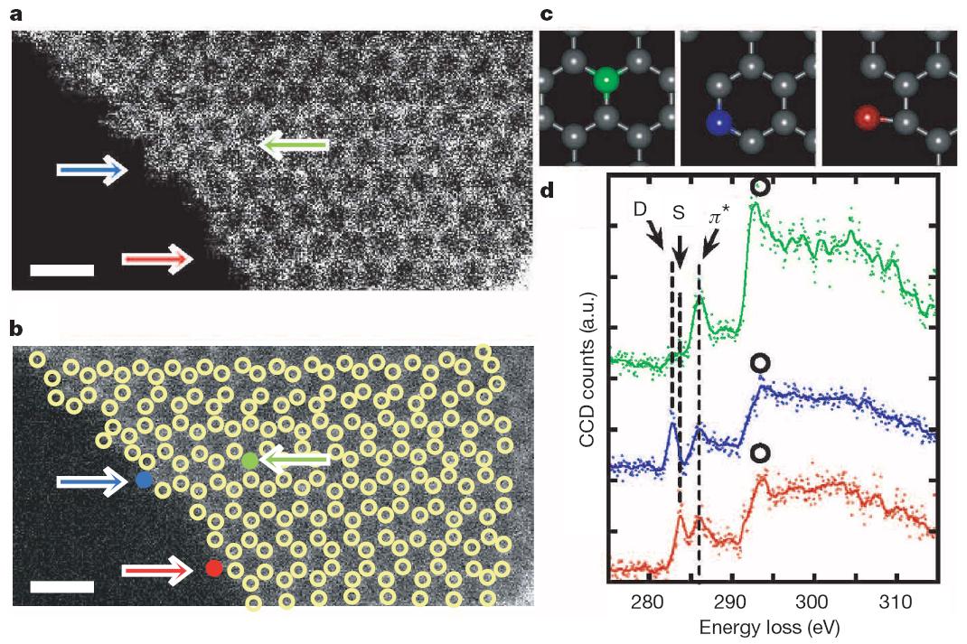
To figure out what exactly happens with atoms at the edges of graphene, Kazu Suenaga and Masanori Koshino from Japan’s National Institute of Advanced Industrial Science and Technology imaged and characterized the electronic properties of single atoms at the edge of graphene with a high-resolution scanning electron microscope. Their findings on how these atoms bond with each other are published this week in Nature.

When it comes to transistors that are smaller than anything that could be done with silicon, graphene is one of the materials of choice. As transistors shrink so much they consist of only a few atoms the electric currents that atomic bonds have to carry can become huge. Only a few materials can sustain this and graphene would be perfect for it. “The bonds between the carbon atoms in graphene are very strong and can carry exceptionally high currents,” Andre Geim told me once when researching a feature on future computing technologies. Moreover, electrons can travel through graphene for long distances, easily comparable to the distance between the source and drain electrical contacts of a transistor. “Your electrons would move between source and drain without scattering,” says Geim.

Characterising individual atoms of graphene. The atoms depicted in red, blue and green colours represent atoms at different positions on a graphene sheet. Their energy loss spectra mirror their different properties. Reprinted by permission from Nature doi: 10.1038/nature09664 (2010).

While all this is true for the centre of graphene sheets, the edges are a different matter. There, electrons scatter and all these nice benefits of graphene are diminished. And the smaller the transistors get the more edges there are in relation to the rest of the surface.

The atoms at the edges of graphene have of course been imaged many times before. What the researchers have now achieved is that they are also able to measure their energy absorption. This leaves a spectral fingerprint on how these atoms are bonded to their neighbours, depending on their position in the atomic structure. The identification of novel electronic states is one of the key findings of their study according to Suenaga. “No one else has ever seen the peaks we report in this work.”

[…]

Continue reading...