This week two interesting papers have been published that I did not get around to highlight here. In terms of topic they could not be more different, one about a possible new data storage material, and the other one about string theory!
The next big thing in computing could be silicon!

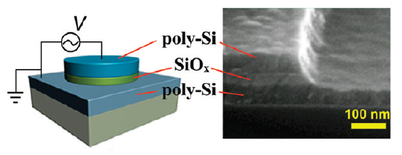
A new memory element made from silicon oxide (SiOx) between two silicon contacts. It promises a silicon-compatible non-volatile memory device. Reprinted with permission from Nano Letters DOI: 10.1021/nl102255r. Copyright 2010 American Chemical Society.
It is not often that advances in condensed matter physics are highlighted on the front page of the New York Times, but the possibility of a new silicon memory technology was compelling enough it seems. The New York Times story is a bit short on details, but one of the authors of the paper published in Nano Letters, Douglas Natelson from Rice University in Houston, describes details of the work on his blog.
What Doug and his colleagues have discovered is that by applying a sufficiently high voltage to an insulating silicon oxide the material suddenly becomes conducting. Increase the voltage further and the devices becomes insulating again. The effect is very pronounced and fully reversible for at least 10,000 cycles. What happens during the initial switching is that electrochemical processes lead to the formation of electrically conducting silicon nanocrystals within the oxide. The nanocrystals are close together so that electrons can easily hop from one to the other so that the device becomes conducting. At even higher voltages the device becomes insulating again as heating effects mean that probably some of the silicon oxidizes again.
The channels between the conducting silicon nanocrystals are only 5 nanometers wide. This suggests that memory devices could be fabricated that are much smaller than present memory devices with sizes of a few tens of nanometers. The device design is really simple. Switching occurs through the application of voltage pulses, which requires only two wires: one input and one output. Moreover, the fabrication of silicon oxide is fully compatible with present silicon technology. And in comparison to the silicon chips in your computer this memory device is non-volatile, it doesn’t lose the information when the computer is turned off. Rather, it behaves more like the flash memory used in solid-state hard drives.
Obviously, a lot of work is required to bring this to the market. At the same time, conceptually this memory effect is somewhat related to that memristor devices. The same New York Times article mentions how Hewlett-Packard is in the process of developing memristor memory chips, so prospects seem realistic.
Reference:
Yao, J., Sun, Z., Zhong, L., Natelson, D., & Tour, J. M. (2010). Resistive Switches and Memories from Silicon Oxide Nano Letters DOI: 10.1021/nl102255r
Could string theory be proven experimentally?

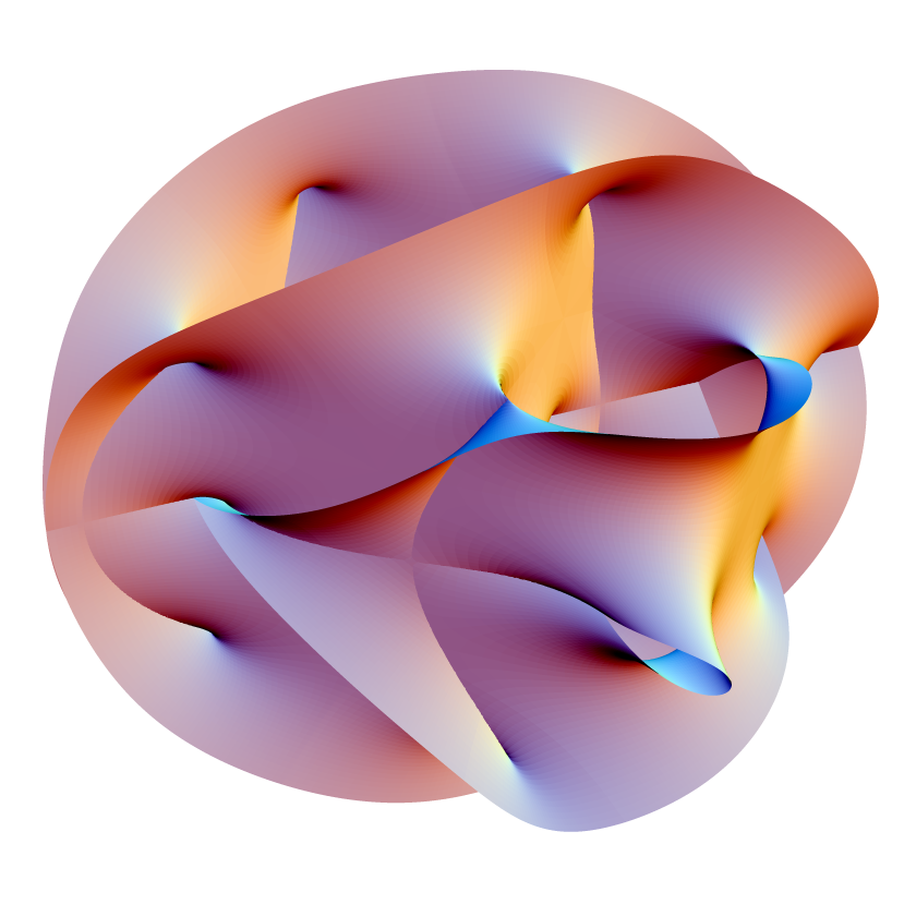
One of the geometrical objects studied in string theory. The image shows a three-dimensional projection of this six-dimensional object. Image by Lunch via Wikimedia Commons.
String theory promises nothing less than to unify the most fundamental concepts in physics, quantum physics and general relativity. In string theory fundamental particles like electrons are not billiard ball-like particles but vibrating strings that can be imagined as little rubber bands.
Unfortunately, string theory is not nearly as straightforward as this simple picture may suggest. The mathematical description of these strings is very challenging and requires more than the four dimensions we know from our universe (space, time). Indeed, most string theories are based on ten-dimensional spaces. To explain the fact that we observe only four of them, one has to imagine the remaining dimensions to be reduced so that they cannot be observed. It is as if you compress a cubic object in one direction until it almost looks like a flat sheet — effectively you see only two dimensions.
One of the biggest problems of string theory is, however, that it cannot be proven experimentally. Or so we thought. In a Physical Review Letters paper Michael Duff and colleagues from Imperial College London claim to have found an experimental proof. They realized that an identical mathematical formulation describes so-called quantum entanglement experiments with single particles of light, photons, as well as black holes. According to the Imperial College press release Duff had this idea at a conference when listening to a talk on entanglement. “I suddenly recognised his formulae as similar to some I had developed a few years earlier while using string theory to describe black holes. When I returned to the UK I checked my notebooks and confirmed that the maths from these very different areas was indeed identical.”
I cannot claim to understand much about Duff’s paper, but it seems that experiments on the entanglement of four photons should be able to replicate certain properties of black holes — if string theory is correct. String theory is controversial, and I am sure this won’t be the last word on the topic. But I am sure somewhere someone is already planning such entanglement experiments. It is too tempting.
Reference:
L. Borsten, D. Dahanayake, M. J. Duff, A. Marrani, & W. Rubens (2010). Four-qubit entanglement from string theory Phys.Rev.Lett.105:100507,2010 arXiv: 1005.4915v2


September 4, 2010
Comments Off on In other news: shrinking computer chips, string theory