November 19, 2012

Comments Off on Graphene’s new look

Graphene’s new look

It’s been only a week ago that I wrote about the increasing competition for graphene. But as I said then, there are still some exciting advances based on graphene. An example is photonics, which is an area where traditionally graphene perhaps has not been as strong as in electronics. A reason for this is that being only a single atomic layer thin, graphene initially wasn’t expected to show much interaction with light. One of the more intriguing historic results in this area has been the fact that the absorption of light in graphene is determined by one of nature’s most fundamental numbers, the fine structure constant.
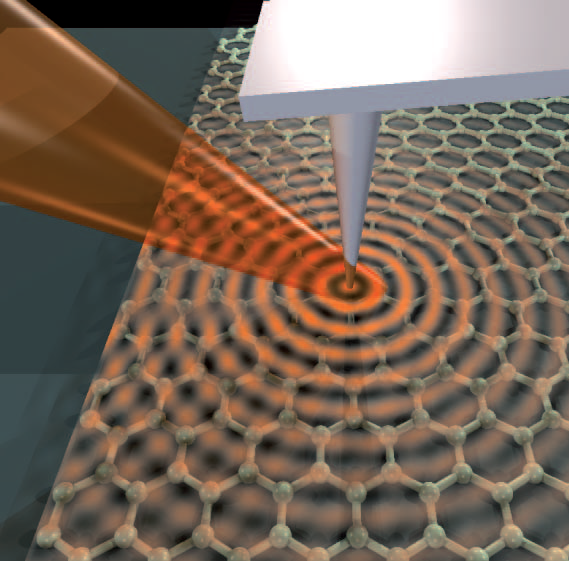
Plasmons in graphene can be created by illuminating the tip of an atomic force microscope (grey) with an infrared laser beam (red). Reprinted by permission from Macmillan Publishers Ltd. Fei Z. et al. Nature 487, 82–85 (2012). doi:10.1038/nature11253

But absorption of light is not where the true potential of graphene lies, namely on the nanoscale. On the same scale as electronic applications, because ultimately the aim is to achieve photonic functionality on a chip.

However, the control of light on the nanoscale typically requires surface plasmons. These are collective movements of electrons at the surface of metals. So in a sense surface plasmons function a bit like antenna that can focus light into tiny spots. Continue reading…

November 13, 2012

2 Comments

Competition in flatland

Move over graphene, there is competition in town. A new type of two-dimensional materials – with the far less appealing family name, transition metal dichalcogenides –  are increasingly gaining attention. Well, at least they’re giving it a shot. Graphene, a sheet of carbon atoms only one atomic layer thick, still has plenty going for itself in terms of electronic, optical and mechanical properties. There seems nothing that graphene can’t do.

On the other hand, there are also limits. When it comes to its electronic properties graphene is not a semiconductor in the same was as silicon is. It is lacking a bandgap, a gap in its electronic states that is important for light emitters and for some electronic devices.

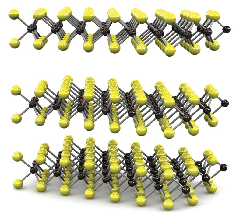
Transition metal dichalcogenide atomic layers

Schematic model of transition metal dichalcogenide atomic layers. The yellow balls represent the chalcogenide atoms, the blue ones the transition metals. Reprinted by permission from Macmillan Publishers Ltd. Nature Nanotechnology (2012). doi:10.1038/nnano.2012.193

Transition metal dichalcogenides offer an advantage there. They are semiconductors, and they can have a bandgap. And as their name says, they are formed by a combination of chalcogens such as sulphur or selenium and transition metals such as molybdenum or tungsten. Typical examples are MoS2 or MoSe2. These materials have become such hot stuff now that their properties have been reviewed in this month’s issue of Nature Nanotechnology. And even though the field is still young, there is plenty to review. Continue reading…

November 8, 2012

Comments Off on The ultimate optical surface devices

The ultimate optical surface devices

Ultrathin coatings for colourful metals

Metals appear colourful by depositing an ultrathin layer of a semiconductor on top. Shown here is the example of thin germanium films on top of gold. Reprinted by permission from Macmillan Publishers Ltd. Nature Materials (2012). doi:10.1038/nmat3443

Ocean waves are pretty relentless when hitting on a beach, and it is not always easy to protect beaches from erosion. For example, if you were to put pillars of a few centimetres in diameter into the water it won’t stop the waves or alter their behaviour. The waves will continue to hit the beach as ever. In optics, the situation is pretty similar. Structures much smaller than the wavelength will have no dramatic effect on a light beam. But as Federico Capasso and his group at Harvard University have shown in a number of papers over the past year, tiny metal structures on the surface of a material can completely alter the way in which light passes through the device. The structures are ultrathin – a few tens of nanometers in height are enough to make exotic types of lenses or to achieve an efficient absorption of the light. Indeed, their approach in designing optical interfaces represents a completely new way of thinking about surfaces, and to me is one of the most exciting developments in photonics this year. Continue reading…