The study of materials is one of the major areas of science, with legions of researchers in physics, chemistry and materials science working on this topic. Condensed matter physics is one of the largest research areas in physics. Yet, it makes me often uneasy how the benefits of materials science are promoted. It is all too often about applications, and not about fundamental physics. How materials such as graphene might revolutionize electronics. And how new physical concepts could be used to develop materials for energy applications: solar cells, batteries and so on. In classical materials science it’s often about tougher materials, such as enhanced steels, and less about the fundamental insights they are based on. Of course, applications are an important aspect in the study of materials. But does this mean that too often fundamental insights are neglected in favour of a material’s commercial potential?
Tag Archives: graphene
The air is getting thinner for silicon’s competitors
May 26, 2011

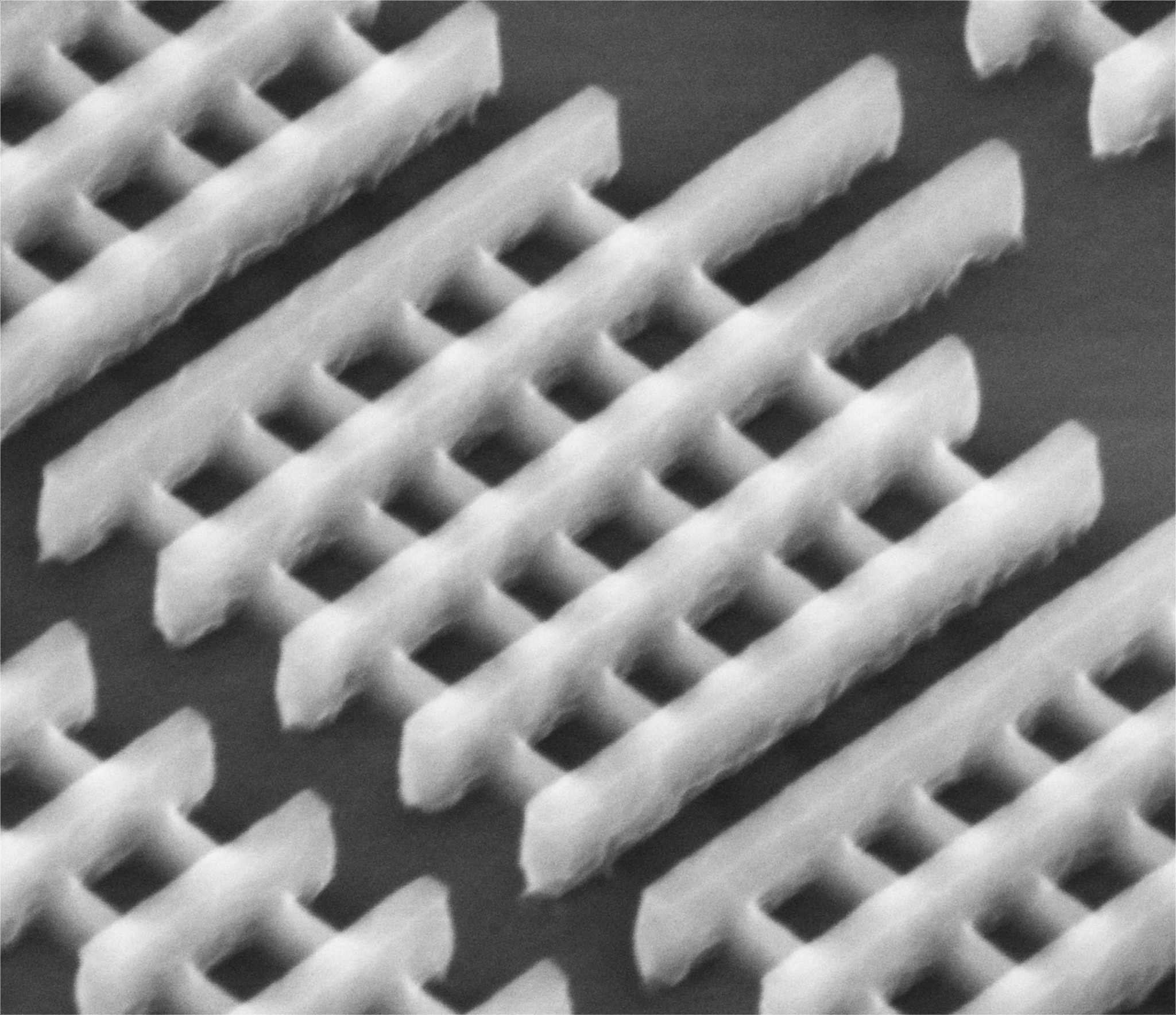
Intel's 3D tri-gate transistors have a feature size of only 22 nm. The thin structures are the silicon channels, the thicker ones are the gates and the contacts. Several gates can be used next to each other to enhance the efficiency of the switching. (c) Intel
Finally I am getting around to blog about the latest generation of transistors that Intel presented earlier this months. These transistors reach feature sizes of only 22 nanometres, down from 32 nm. To give you some perspective what this amazingly high integration means: 4,000 of those 22 nm structures fit across the width of a human hair, or similarly, 100 million of these transistors fit on the head of a pin.
Now how did they reduce transistor length scales down by almost a third? Well, even though Intel (and others) is in the business of shrinking transistor for more than 40 years, this time it’s a bit more than a mere scaling exercise. For the first time we have a commercial 3D transistor design on such a scale. In a typical ‘field-effect’ transistor, two electrical contacts are used to run an electric current through a silicon layer. The transistor is switched between an electrically conducting and an insulating state by a gate on top of the silicon. The voltage applied to that gate determines whether current can flow or not. Thereby the gate is able to set the digital ‘1’ and ‘0’ in a transistor.
A problem in shrinking transistors has been the fact that those three electric contacts need a certain minimum space of their own. Furthermore, as the gate has become smaller and smaller, it has been increasingly inefficient to switch the electric current in the silicon layer underneath. For smaller gates the electric fields from the gate just don’t reach that far down into the silicon layer. […]
2010 – twelve months of great science
December 27, 2010
The past year has been a great year for science with major advances in several areas. Too many exciting results to mention here. Instead, to reflect about the past year I have chosen a representative paper for each month of the year that I hope can serve as an example of the great science going on in a number of research fields. Of course, this is a highly subjective and personal collection, and indeed there might be others worth mentioning. But the aim was also to provide a balanced overview of the year that covers a variety of topics.
Of course, if you have an exciting paper to add, please feel free to use the comments section below to let us know!
Anyway, enough said, here are some of my highlights from the past year:

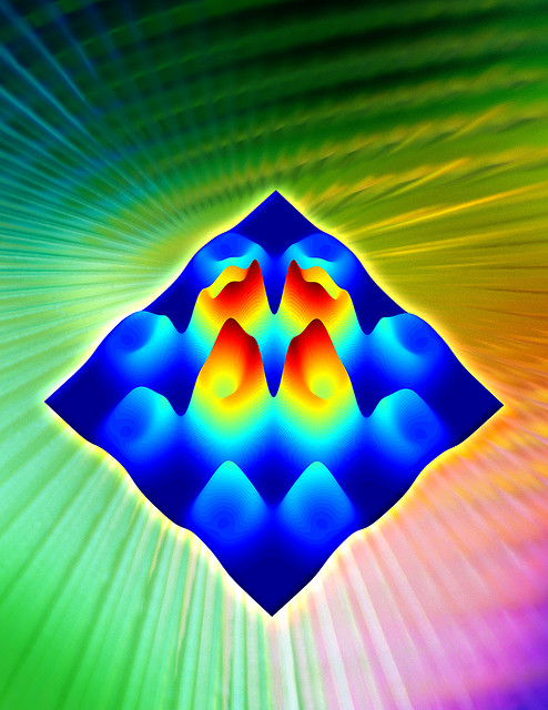
Simulations of electronic excitations in an iron-based superconductor. Image by Oak Ridge National Laboratory via flickr.
JANUARY – iron-based superconductors
Since they were discovered in 2008, iron-based superconductors, the pnictides, have been one of the hottest topics in condensed matter physics. Part of their appeal stems from the fact that they are based on iron, which is a magnetic element. Normally, magnets and superconductivity exclude each other.
The iron-based compounds have a similar crystal structure as the so-called cuprates, which are the materials with the highest superconducting temperatures known. The mechanism for these high-temperature superconductors is unknown, and studying the iron-based superconductors may also be relevant to the understanding of the cuprates.
This paper published in Science shows for the first time that the electrons in the iron-based superconductors show a periodic arrangement that is different to the periodicity of the atoms in the crystal. Similar observations have been made in the cuprates, and their understanding is considered important to the mechanism of high-temperature superconductivity.
Chuang, T., Allan, M., Lee, J., Xie, Y., Ni, N., Bud’ko, S., Boebinger, G., Canfield, P., & Davis, J. (2010). Nematic Electronic Structure in the “Parent” State of the Iron-Based Superconductor Ca(Fe1-xCox)2As2 Science, 327 (5962), 181-184 DOI: 10.1126/science.1181083


November 7, 2011
5 Comments