Tag Archives: graphene

Graphene on the edge

December 15, 2010

Comments Off on Graphene on the edge

Following this year’s Nobel prize in physics to Andre Geim and Konstantin Novoselov, the relevance of graphene hardly needs to be stated. Graphene-based devices have a real potential owing to the material’s unique electronic properties. If graphene, which is metallic, is cut into small pieces it becomes semiconducting and could be used as a transistor. The problem is however the edges of such small graphene devices. These perturb the operation of graphene transistors, and this is the reason one has to be cautious when it comes to immediate relevance for applications.

To figure out what exactly happens with atoms at the edges of graphene, Kazu Suenaga and Masanori Koshino from Japan’s National Institute of Advanced Industrial Science and Technology imaged and characterized the electronic properties of single atoms at the edge of graphene with a high-resolution scanning electron microscope. Their findings on how these atoms bond with each other are published this week in Nature.

When it comes to transistors that are smaller than anything that could be done with silicon, graphene is one of the materials of choice. As transistors shrink so much they consist of only a few atoms the electric currents that atomic bonds have to carry can become huge. Only a few materials can sustain this and graphene would be perfect for it. “The bonds between the carbon atoms in graphene are very strong and can carry exceptionally high currents,” Andre Geim told me once when researching a feature on future computing technologies. Moreover, electrons can travel through graphene for long distances, easily comparable to the distance between the source and drain electrical contacts of a transistor. “Your electrons would move between source and drain without scattering,” says Geim.
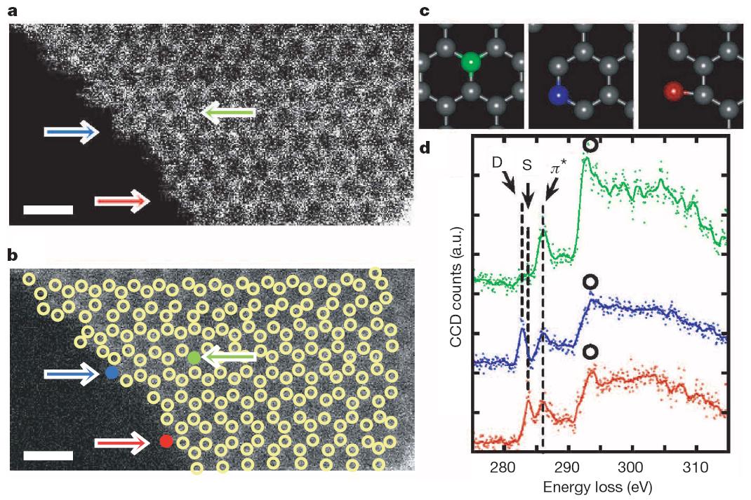
Characterising individual atoms of graphene. The atoms depicted in red, blue and green colours represent atoms at different positions on a graphene sheet. Their energy loss spectra mirror their different properties. Reprinted by permission from Nature doi: 10.1038/nature09664 (2010).

While all this is true for the centre of graphene sheets, the edges are a different matter. There, electrons scatter and all these nice benefits of graphene are diminished. And the smaller the transistors get the more edges there are in relation to the rest of the surface.

The atoms at the edges of graphene have of course been imaged many times before. What the researchers have now achieved is that they are also able to measure their energy absorption. This leaves a spectral fingerprint on how these atoms are bonded to their neighbours, depending on their position in the atomic structure. The identification of novel electronic states is one of the key findings of their study according to Suenaga. “No one else has ever seen the peaks we report in this work.”

[…]

Continue reading...

Great, the physics Nobel prize for graphene! Now don’t overhype it…

October 5, 2010

29 Comments

Today it was announced that the 2010 Nobel prize in physics goes to Andre Geim and Konstantin Novoselovfor groundbreaking experiments regarding the two-dimensional material graphene.”

Geim’s and Novoselov’s work on graphene has been frequently predicted for the Nobel prize, although interestingly graphene has been studied long before they entered the field. Studies on graphene go back at least to the 1970s, and the name for this atomically thin layer of carbon came into more wider use in the 1980s.

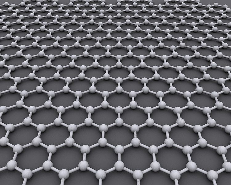
A model of graphene. Image by AlexanderAlUS via Wikimedia Commons.

So what is the big deal with Geim’s and Novoselov’s research? Well, they developed a really simple method to fabricate graphene. Graphene is a close relative of graphite. Graphite consists of layers of carbon where in each layer the carbon atoms arrange as hexagons. These layers can be visualized as sheets of chicken wire.

Graphene is nothing but a single one of those sheets that make up graphite. The method Geim and Novoselov developed in 2004 to extract graphene is stunningly simple. Take a graphite pencil and write with it on a piece of paper. Then take a post-it note and use it to lift off tiny pieces of graphite. Look under the microscope and identify the single layer ones, and that’s it! But of course, in the meantime more efficient fabrication technologies for graphene have been developed.

As Geim, Novoselov, and many others consequently demonstrated, graphene is a unique material, fundamentally different to graphite. It is highly conducting, and electrons can travel through it for long distances without being deflected. This makes it interesting for fast transistors, and this is the point also of Geim and Novoselov’s ground-breaking first paper on graphene published in Science in 2004. Graphene shows also some interesting electronic properties owing to its electronic band structure, even the fractional quantum Hall effect.

And then of course the electronic bonds in graphene are very strong, which not unlike carbon nanotubes makes it an excellent structural material. Then there are possible applications in molecular sensing and many others. All this makes graphene highly interesting for researchers from many scientific areas. However, some of the rationale expressed by the Nobel Committee strikes me a bit odd, evidenced by this tweet: “According to Nobel Committee, practical applications for graphene include touch screens, fast transistors & DNA sequencing. #nobelprize.”

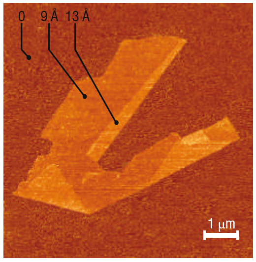
Flakes of graphene. Reprinted by permission from Macmillan Publishers Ltd. Nature Materials 6, 183-191 (2007).

Indeed, I agree that graphene has potential in all these areas. But we still have to see those promised applications. The last application in this list, DNA sequencing, is from a Nature paper less than a month old!

As for transistors, well, the edges of graphene cause a lot of problem, and so does fabrication. I recently blogged about attempts to use nanowires to make graphene transistors, which are still very far off commercial uses as well. And when it comes to the band structure properties of graphene such as the so-called Dirac point, well, topological insulators show similar physics but could be far more promising.

Graphene is a highly interesting and versatile material with cool properties. But when it comes to applications, well, we will see whether an all-rounder such as graphene will be able to beat incumbents. This is certainly far from clear yet. So please let’s stay realistic on the practical implications of graphene.

Overall of course, I am very happy for Geim and Novoselov, they certainly deserve the prize. At the same time I find it interesting that Sumio Iijima‘s discovery of carbon nanotubes hasn’t been rewarded yet.

In any case, it is a great week for UK science, with Nobel prizes in medicine and physics going to UK institutions. This recognition shows the high standard of UK science, which is presently in severe danger from government budget cuts.

Reference:
Novoselov, K., & Geim, A. (2004). Electric Field Effect in Atomically Thin Carbon Films Science, 306 (5696), 666-669 DOI: 10.1126/science.1102896

Further reading:
Geim, A., & Novoselov, K. (2007). The rise of graphene Nature Materials, 6 (3), 183-191 DOI: 10.1038/nmat1849

This post was chosen as an Editor's Selection for ResearchBlogging.org This post was chosen as an Editor’s Selection for ResearchBlogging.org

Continue reading...

Yet more graphene transistors – it’s twins!

September 8, 2010

1 Comment

Last week I blogged about a Nature paper on graphene transistors with a self-aligned nanowire gate.  Well, as I gather from a blog post by Doug Natelson, largely the same UCLA researchers have now published a paper in Nano Letters that uses a rather similar idea, even though in the latest paper the nanowire gate is made from another material, and it seems the latest transistors are even faster.

However, I am worried about the obviously parallel publication of these two papers. The Nature paper was submitted 23 May, published 1 September. The Nano Letters paper was submitted 16 May and published 3 September.

As Doug says: “Looks like they managed to get two papers in good journals for the price of one technique advance.” And I agree, it looks very much like salami slicing of research results to me. In particular, I like to emphasize that it is editorial policy of Nature journals that editors (like myself) are informed about any related submission made to other journals — see Nature‘s policy on duplicate submissions and plagiarism.

I have not checked this fact with my colleagues and if I would have I could not comment here on my private blog, but I do wonder whether such communication has taken place here. If I were the handling editor, this dual publication would not have been knowingly possible, but others might of course have a different opinion.

Either way, in cases where our policy on duplicate submission is not followed, little can be done if clearly different materials were used, even if a study is based on a similar concept. Apart from increased scrutiny of such authors in future submissions of course.

References:

Liao, L., Bai, J., Cheng, R., Lin, Y., Jiang, S., Qu, Y., Huang, Y., & Duan, X. (2010). Sub-100 nm Channel Length Graphene Transistors Nano Letters DOI: 10.1021/nl101724k

Liao, L., Lin, Y., Bao, M., Cheng, R., Bai, J., Liu, Y., Qu, Y., Wang, K., Huang, Y., & Duan, X. (2010). High-speed graphene transistors with a self-aligned nanowire gate Nature DOI: 10.1038/nature09405

Continue reading...