Tag Archives: nanowires

The air is getting thinner for silicon’s competitors

May 26, 2011

9 Comments

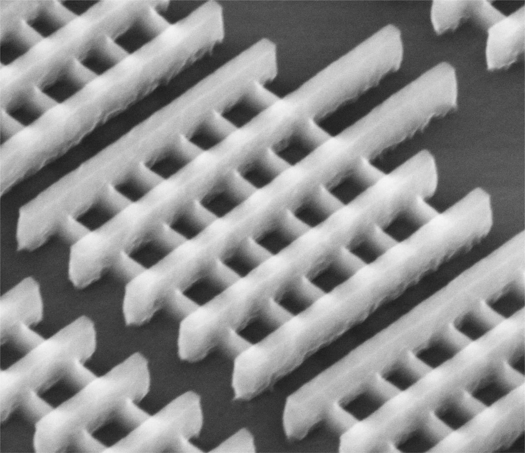
Intel's 3D tri-gate transistors have a feature size of only 22 nm. The thin structures are the silicon channels, the thicker ones are the gates and the contacts. Several gates can be used next to each other to enhance the efficiency of the switching. (c) Intel

Finally I am getting around to blog about the latest generation of transistors that Intel presented earlier this months. These transistors reach feature sizes of only 22 nanometres, down from 32 nm. To give you some perspective what this amazingly high integration means: 4,000 of those 22 nm structures fit across the width of a human hair, or similarly, 100 million of these transistors fit on the head of a pin.

Now how did they reduce transistor length scales down by almost a third? Well, even though Intel (and others) is in the business of shrinking transistor for more than 40 years, this time it’s a bit more than a mere scaling exercise. For the first time we have a commercial 3D transistor design on such a scale. In a typical ‘field-effect’ transistor, two electrical contacts are used to run an electric current through a silicon layer. The transistor is switched between an electrically conducting and an insulating state by a gate on top of the silicon. The voltage applied to that gate determines whether current can flow or not. Thereby the gate is able to set the digital ‘1’ and ‘0’ in a transistor.

A problem in shrinking transistors has been the fact that those three electric contacts need a certain minimum space of their own. Furthermore, as the gate has become smaller and smaller, it has been increasingly inefficient to switch the electric current in the silicon layer underneath. For smaller gates the electric fields from the gate just don’t reach that far down into the silicon layer. […]

Continue reading...

Yet more graphene transistors – it’s twins!

September 8, 2010

1 Comment

Last week I blogged about a Nature paper on graphene transistors with a self-aligned nanowire gate.  Well, as I gather from a blog post by Doug Natelson, largely the same UCLA researchers have now published a paper in Nano Letters that uses a rather similar idea, even though in the latest paper the nanowire gate is made from another material, and it seems the latest transistors are even faster.

However, I am worried about the obviously parallel publication of these two papers. The Nature paper was submitted 23 May, published 1 September. The Nano Letters paper was submitted 16 May and published 3 September.

As Doug says: “Looks like they managed to get two papers in good journals for the price of one technique advance.” And I agree, it looks very much like salami slicing of research results to me. In particular, I like to emphasize that it is editorial policy of Nature journals that editors (like myself) are informed about any related submission made to other journals — see Nature‘s policy on duplicate submissions and plagiarism.

I have not checked this fact with my colleagues and if I would have I could not comment here on my private blog, but I do wonder whether such communication has taken place here. If I were the handling editor, this dual publication would not have been knowingly possible, but others might of course have a different opinion.

Either way, in cases where our policy on duplicate submission is not followed, little can be done if clearly different materials were used, even if a study is based on a similar concept. Apart from increased scrutiny of such authors in future submissions of course.

References:

Liao, L., Bai, J., Cheng, R., Lin, Y., Jiang, S., Qu, Y., Huang, Y., & Duan, X. (2010). Sub-100 nm Channel Length Graphene Transistors Nano Letters DOI: 10.1021/nl101724k

Liao, L., Lin, Y., Bao, M., Cheng, R., Bai, J., Liu, Y., Qu, Y., Wang, K., Huang, Y., & Duan, X. (2010). High-speed graphene transistors with a self-aligned nanowire gate Nature DOI: 10.1038/nature09405

Continue reading...

The thing with graphene transistors

September 1, 2010

6 Comments

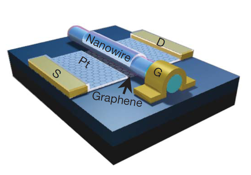
Graphene is one of the hottest research areas in nanotechnology, and it may seem slightly surprising it took me a month to write my first blog post on the topic. That moment has now come, with the advance publication of a Nature paper that presents highly attractive graphene transistor, even though in my humble opinion the approach taken seems not the most promising for future highly integrated devices.

There are many reasons why graphene gets researchers so excited. The stability of this single layer of carbon atoms is one of the reasons, promising tough composite materials with increased mechanical strength. The unusual electronic properties that in some respect resemble that of relativistic particles is another. And last but not least, the fact that electrons can travel ballistic, without hitting carbon atoms, for long distances in the micrometer range is another. All these contribute to graphene’s success.

Schematic of the device where a nanowire acts as gate for a graphene transistor. Reprinted by permission from Macmillan Publishers Ltd. Nature (2010). doi:10.1038/nature09405

Two years ago I wrote a feature in New Scientist where I focussed on the potential of graphene to replace silicon logic. The piece is now behind a pay wall, but when talking to Andre Geim at the time, a pioneer in the field, he told me that graphene is uniquely suited to scale down to device dimensions impossible to achieve with silicon. Any transistor needs to support an electric current, that is how you read out its status. However, if you shrink the size of a transistor to only a few nanometers, this electric current will flow across only a small number of atomic bonds. Silicon bonds might not be able to sustain such high current densities. Not so graphene. “The bonds between the carbon atoms in graphene are very strong and can carry exceptionally high currents,” said Geim back then.

[…]

Continue reading...