It’s been only a week ago that I wrote about the increasing competition for graphene. But as I said then, there are still some exciting advances based on graphene. An example is photonics, which is an area where traditionally graphene perhaps has not been as strong as in electronics. A reason for this is that being only a single atomic layer thin, graphene initially wasn’t expected to show much interaction with light. One of the more intriguing historic results in this area has been the fact that the absorption of light in graphene is determined by one of nature’s most fundamental numbers, the fine structure constant.
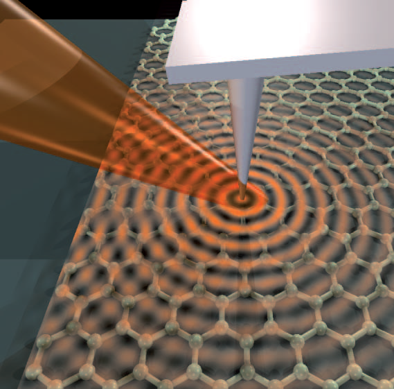
Plasmons in graphene can be created by illuminating the tip of an atomic force microscope (grey) with an infrared laser beam (red). Reprinted by permission from Macmillan Publishers Ltd. Fei Z. et al. Nature 487, 82–85 (2012). doi:10.1038/nature11253
But absorption of light is not where the true potential of graphene lies, namely on the nanoscale. On the same scale as electronic applications, because ultimately the aim is to achieve photonic functionality on a chip.
However, the control of light on the nanoscale typically requires surface plasmons. These are collective movements of electrons at the surface of metals. So in a sense surface plasmons function a bit like antenna that can focus light into tiny spots. […]
Continue reading...

Hydrogen sensing at the nanoscale. Hydrogen molecules (red) are absorbed by a palladium nanoparticle (silver) and the resulting changes in optical properties amplified by a gold antenna. (c) Mario Hentschel, Na Liu, Harald Giessen
Sensing the presence of molecules in gases and liquids is a billion dollar business. Just think about all the carbon monoxide detectors in private homes, or blood glucose sensors. In particular for many technical and scientific applications, ultrasmall and precise sensors are desired. This includes sensors to measure gases in catalytic nanoreactors and fuel cells, or the monitoring of biochemical processes.
Laura Na Liu and Ming Tang from the group of Paul Alivisatos, director of Lawrence Berkeley Lab in the USA, and Mario Hentschel from Harald Giessen‘s group at the University of Stuttgart in Germany have now developed a new class of optical nanoscale sensors that are able to measure specific molecular concentrations down to single particles. This, says Alivisatos, “should pave the road for the optical observation of chemical reactions and catalytic activities in nanoreactors, and for local biosensing.” Their paper is published this week in Nature Materials (declaration of interest: I was the handling editor of this paper, although I like to stress that I don’t benefit in my day job by blogging about this work). […]
Continue reading...
How do you measure a field like electrical or magnetic fields? The field itself is of course not visible. But you can see the effects of a field and use that for the visualization. For example, in case of magnetic fields a nice high school type of experiment is to use iron filings sprayed around a magnet. The filings align along the field lines (so that the force on them is minimum), and this alignment makes the field lines visible.
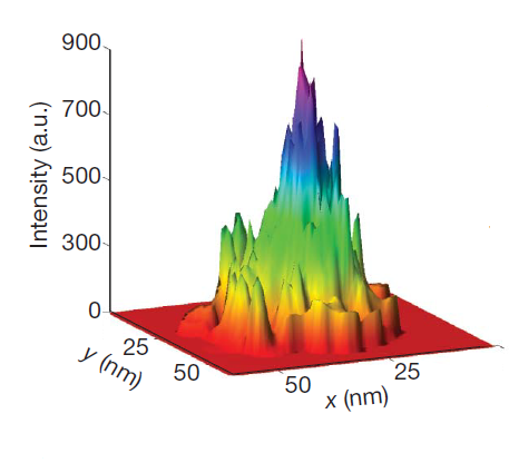
The electromagnetic fields of a hot spot on the surface of aluminium. The hotspot is only a few nanometres in size. (c) Nature Publishing Group. Nature 469, 385-389 (2011).
Although this kind of visualization technique works very well for larger objects, things get trickier if the fields are concentrated within the tiniest spots only a few nanometers large. There aren’t many objects that could be used to measure fields on that scale. Yet Xiang Zhang and colleagues from the University of Berkeley have achieved exactly that and developed a method capable of measuring the electromagnetic fields down to an area only 15 nanometres in size.
The fields they measure are so-called hotspots that form at the surface of metals or around metallic nanostructures such as nanoparticles or nanoscale bow tie structures. There, collective movements of the electrons – the surface plasmons – can create huge electromagnetic fields. This is very much in analogy to the way any other antenna works: oscillating electrical currents create electromagnetic radio waves. On the surface of metal nanostructures, the same happens; but because the geometry is so small the effect is much larger.
[…]
Continue reading...


November 19, 2012
Comments Off on Graphene’s new look