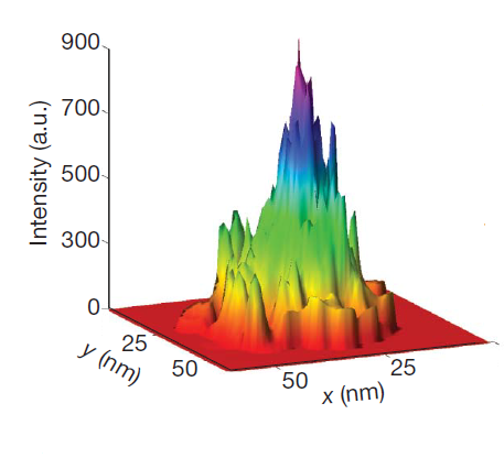
How do you measure a field like electrical or magnetic fields? The field itself is of course not visible. But you can see the effects of a field and use that for the visualization. For example, in case of magnetic fields a nice high school type of experiment is to use iron filings sprayed around a magnet. The filings align along the field lines (so that the force on them is minimum), and this alignment makes the field lines visible.

The electromagnetic fields of a hot spot on the surface of aluminium. The hotspot is only a few nanometres in size. (c) Nature Publishing Group. Nature 469, 385-389 (2011).
Although this kind of visualization technique works very well for larger objects, things get trickier if the fields are concentrated within the tiniest spots only a few nanometers large. There aren’t many objects that could be used to measure fields on that scale. Yet Xiang Zhang and colleagues from the University of Berkeley have achieved exactly that and developed a method capable of measuring the electromagnetic fields down to an area only 15 nanometres in size.
The fields they measure are so-called hotspots that form at the surface of metals or around metallic nanostructures such as nanoparticles or nanoscale bow tie structures. There, collective movements of the electrons – the surface plasmons – can create huge electromagnetic fields. This is very much in analogy to the way any other antenna works: oscillating electrical currents create electromagnetic radio waves. On the surface of metal nanostructures, the same happens; but because the geometry is so small the effect is much larger.


January 20, 2011
1 Comment